- 您现在的位置:买卖IC网 > PDF目录12027 > ADUC814BRUZ (Analog Devices Inc)IC ADC 12BIT W/FLASH MCU 28TSSOP PDF资料下载
参数资料
| 型号: | ADUC814BRUZ |
| 厂商: | Analog Devices Inc |
| 文件页数: | 24/72页 |
| 文件大小: | 0K |
| 描述: | IC ADC 12BIT W/FLASH MCU 28TSSOP |
| 标准包装: | 50 |
| 系列: | MicroConverter® ADuC8xx |
| 核心处理器: | 8052 |
| 芯体尺寸: | 8-位 |
| 速度: | 16.78MHz |
| 连通性: | I²C,SPI,UART/USART |
| 外围设备: | POR,PSM,温度传感器,WDT |
| 输入/输出数: | 17 |
| 程序存储器容量: | 8KB(8K x 8) |
| 程序存储器类型: | 闪存 |
| EEPROM 大小: | 640 x 8 |
| RAM 容量: | 256 x 8 |
| 电压 - 电源 (Vcc/Vdd): | 2.7 V ~ 5.5 V |
| 数据转换器: | A/D 6x12b; D/A 2x12b |
| 振荡器型: | 内部 |
| 工作温度: | -40°C ~ 125°C |
| 封装/外壳: | 28-TSSOP(0.173",4.40mm 宽) |
| 包装: | 管件 |
| 产品目录页面: | 738 (CN2011-ZH PDF) |
| 配用: | EVAL-ADUC814QSZ-ND - KIT DEV FOR ADUC814 MICROCONVRTR |
第1页第2页第3页第4页第5页第6页第7页第8页第9页第10页第11页第12页第13页第14页第15页第16页第17页第18页第19页第20页第21页第22页第23页当前第24页第25页第26页第27页第28页第29页第30页第31页第32页第33页第34页第35页第36页第37页第38页第39页第40页第41页第42页第43页第44页第45页第46页第47页第48页第49页第50页第51页第52页第53页第54页第55页第56页第57页第58页第59页第60页第61页第62页第63页第64页第65页第66页第67页第68页第69页第70页第71页第72页
ADuC814
Rev. A | Page 30 of 72
NONVOLITILE FLASH/EE MEMORY
FLASH/EE MEMORY OVERVIEW
The ADuC814 incorporates Flash/EE memory technology on-
chip to provide the user with nonvolatile, in-circuit reprogram-
mable code and data memory space.
Flash/EE memory takes the flexible in-circuit reprogrammable
features of EEPROM and combines them with the space efficient/
density features of EPROM (see Figure 32).
Because Flash/EE technology is based on a single transistor cell
architecture, a Flash memory array such as EPROM can be
implemented to achieve the space efficiencies or memory
densities required by a given design.
Like EEPROM, flash memory can be programmed in-system at
a byte level, although it must first be erased; the erase being
performed in page blocks. Thus, flash memory is often and
more correctly referred to as Flash/EE memory.
EEPROM
TECHNOLOGY
EPROM
TECHNOLOGY
FLASH/EE MEMORY
TECHNOLOGY
IN-CIRCUIT
REPROGRAMMABLE
SPACE EFFICIENT/
DENSITY
02748-A
-038
Figure 32. Flash/EE Memory Development
Incorporated in the ADuC814, Flash/EE memory technology
allows the user to update program code space in-circuit without
the need to replace one-time programmable (OTP) devices at
remote operating nodes.
FLASH/EE MEMORY AND THE ADUC814
The ADuC814 provides two arrays of Flash/EE memory for
user applications. There are 8 kbytes of Flash/EE program space
provided on-chip to facilitate code execution, therefore removing
the requirement for an external discrete ROM device. The pro-
gram memory can be programmed using conventional third-
party memory programmers. This array can also be programmed
in-circuit, using the serial download mode provided.
A 640-byte Flash/EE data memory space is also provided on-
chip. This may be used as a general-purpose nonvolatile
scratchpad area. User access to this area is via a group of six
SFRs. This space can be programmed at a byte level, although it
must first be erased in 4-byte pages.
ADUC814 FLASH/EE MEMORY RELIABILITY
The Flash/EE program and data memory arrays on the
ADuC814 are fully qualified for two key Flash/EE memory
characteristics: Flash/EE memory cycling endurance and
Flash/EE memory data retention.
Endurance quantifies the ability of the Flash/EE memory to be
cycled through many program, read, and erase cycles. In real
terms, a single endurance cycle is composed of four
independent, sequential events:
1.
Initial page erase sequence
2.
Read/verify sequence
3.
Byte program sequence
4.
Second read/verify sequence
In reliability qualification, every byte in both the program and
data Flash/EE memory is cycled from 00H to FFH until a first
fail is recorded signifying the endurance limit of the on-chip
Flash/EE memory.
As indicated in the Specifications tables, the ADuC814 Flash/EE
memory endurance qualification has been carried out in accor-
dance with JEDEC Specification A117 over the industrial
temperature range of –40°C to +125°C. The results allow the
specification of a minimum endurance figure over supply and a
temperature of 100,000 cycles, with an endurance figure of
700,000 cycles being typical of operation at 25°C.
Retention quantifies the ability of the Flash/EE memory to
retain its programmed data over time. Again, the ADuC814 has
been qualified in accordance with the formal JEDEC Retention
Lifetime Specification (A117) at a specific junction temperature
(TJ = 55°C). As part of this qualification procedure, the Flash/EE
memory is cycled to its specified endurance limit described
above, before data retention is characterized. This means that
the Flash/EE memory is guaranteed to retain its data for its full
specified retention lifetime every time the Flash/EE memory is
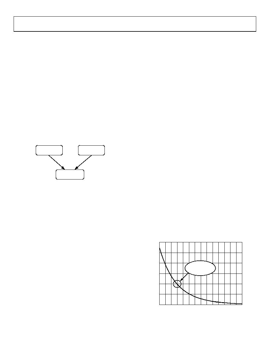
reprogrammed. It should be noted that retention lifetime, based
on an activation energy of 0.6 eV, derates with TJ as shown in
40
60
70
90
TJ JUNCTION TEMPERATURE (°C)
RE
TE
NTION
(Y
e
a
rs
)
250
200
150
100
50
0
50
80
110
300
100
ADI SPECIFICATION
100 YEARS MIN.
AT TJ = 55°C
02748-A
-039
Figure 33. Flash/EE Memory Data Retention
相关PDF资料 |
PDF描述 |
|---|---|
| AT32UC3C064C-ALUT | IC MCU AVR32 64K FLASH 144LQFP |
| VI-J1Z-IW-F4 | CONVERTER MOD DC/DC 2V 40W |
| ADUC7029BBCZ62I | IC MCU 12BIT 62KB FLASH 49BGA |
| VI-B2L-IY-F2 | CONVERTER MOD DC/DC 28V 50W |
| VJ2225A392KBAAT4X | CAP CER 3900PF 50V 10% NP0 2225 |
相关代理商/技术参数 |
参数描述 |
|---|---|
| ADUC814BRUZ-REEL | 功能描述:IC MCU 8K FLASH ADC/DAC 28-TSSOP RoHS:是 类别:集成电路 (IC) >> 嵌入式 - 微控制器, 系列:MicroConverter® ADuC8xx 标准包装:38 系列:Encore!® XP® 核心处理器:eZ8 芯体尺寸:8-位 速度:5MHz 连通性:IrDA,UART/USART 外围设备:欠压检测/复位,LED,POR,PWM,WDT 输入/输出数:16 程序存储器容量:4KB(4K x 8) 程序存储器类型:闪存 EEPROM 大小:- RAM 容量:1K x 8 电压 - 电源 (Vcc/Vdd):2.7 V ~ 3.6 V 数据转换器:- 振荡器型:内部 工作温度:-40°C ~ 105°C 封装/外壳:20-SOIC(0.295",7.50mm 宽) 包装:管件 其它名称:269-4116Z8F0413SH005EG-ND |
| ADUC814BRUZ-REEL7 | 功能描述:IC MCU 8K FLASH ADC/DAC 28-TSSOP RoHS:是 类别:集成电路 (IC) >> 嵌入式 - 微控制器, 系列:MicroConverter® ADuC8xx 标准包装:38 系列:Encore!® XP® 核心处理器:eZ8 芯体尺寸:8-位 速度:5MHz 连通性:IrDA,UART/USART 外围设备:欠压检测/复位,LED,POR,PWM,WDT 输入/输出数:16 程序存储器容量:4KB(4K x 8) 程序存储器类型:闪存 EEPROM 大小:- RAM 容量:1K x 8 电压 - 电源 (Vcc/Vdd):2.7 V ~ 3.6 V 数据转换器:- 振荡器型:内部 工作温度:-40°C ~ 105°C 封装/外壳:20-SOIC(0.295",7.50mm 宽) 包装:管件 其它名称:269-4116Z8F0413SH005EG-ND |
| ADUC816 | 制造商:未知厂家 制造商全称:未知厂家 功能描述:ADuC816: MicroConverter?= Dual 16-Bit ADC + 12-Bit DAC + Flash MCU Data Sheet (Rev. 0. 2/01 |
| ADUC816ASZ | 功能描述:8052 MicroConverter? ADuC8xx Microcontroller IC 8-Bit 12.58MHz 8KB (8K x 8) FLASH 制造商:analog devices inc. 系列:MicroConverter? ADuC8xx 包装:- 零件状态:上次购买时间 核心处理器:8052 核心尺寸:8-位 速度:12.58MHz 连接性:I2C,SPI,UART/USART 外设:PSM,温度传感器,WDT I/O 数:34 程序存储容量:8KB(8K x 8) 程序存储器类型:闪存 EEPROM 容量:640 x 8 RAM 容量:256 x 8 电压 - 电源(Vcc/Vdd):2.7 V ~ 5.5 V 数据转换器:A/D 7x16b;D/A 1x12b 振荡器类型:内部 工作温度:-40°C ~ 85°C(TA) 封装/外壳:- 供应商器件封装:- 标准包装:1 |
| ADUC816BCP | 功能描述:IC MCU 8K FLASH ADC/DAC 56LFCSP RoHS:否 类别:集成电路 (IC) >> 嵌入式 - 微控制器, 系列:MicroConverter® ADuC8xx 标准包装:38 系列:Encore!® XP® 核心处理器:eZ8 芯体尺寸:8-位 速度:5MHz 连通性:IrDA,UART/USART 外围设备:欠压检测/复位,LED,POR,PWM,WDT 输入/输出数:16 程序存储器容量:4KB(4K x 8) 程序存储器类型:闪存 EEPROM 大小:- RAM 容量:1K x 8 电压 - 电源 (Vcc/Vdd):2.7 V ~ 3.6 V 数据转换器:- 振荡器型:内部 工作温度:-40°C ~ 105°C 封装/外壳:20-SOIC(0.295",7.50mm 宽) 包装:管件 其它名称:269-4116Z8F0413SH005EG-ND |
发布紧急采购,3分钟左右您将得到回复。