- 您现在的位置:买卖IC网 > PDF目录12027 > ADUC814BRUZ (Analog Devices Inc)IC ADC 12BIT W/FLASH MCU 28TSSOP PDF资料下载
参数资料
| 型号: | ADUC814BRUZ |
| 厂商: | Analog Devices Inc |
| 文件页数: | 59/72页 |
| 文件大小: | 0K |
| 描述: | IC ADC 12BIT W/FLASH MCU 28TSSOP |
| 标准包装: | 50 |
| 系列: | MicroConverter® ADuC8xx |
| 核心处理器: | 8052 |
| 芯体尺寸: | 8-位 |
| 速度: | 16.78MHz |
| 连通性: | I²C,SPI,UART/USART |
| 外围设备: | POR,PSM,温度传感器,WDT |
| 输入/输出数: | 17 |
| 程序存储器容量: | 8KB(8K x 8) |
| 程序存储器类型: | 闪存 |
| EEPROM 大小: | 640 x 8 |
| RAM 容量: | 256 x 8 |
| 电压 - 电源 (Vcc/Vdd): | 2.7 V ~ 5.5 V |
| 数据转换器: | A/D 6x12b; D/A 2x12b |
| 振荡器型: | 内部 |
| 工作温度: | -40°C ~ 125°C |
| 封装/外壳: | 28-TSSOP(0.173",4.40mm 宽) |
| 包装: | 管件 |
| 产品目录页面: | 738 (CN2011-ZH PDF) |
| 配用: | EVAL-ADUC814QSZ-ND - KIT DEV FOR ADUC814 MICROCONVRTR |
第1页第2页第3页第4页第5页第6页第7页第8页第9页第10页第11页第12页第13页第14页第15页第16页第17页第18页第19页第20页第21页第22页第23页第24页第25页第26页第27页第28页第29页第30页第31页第32页第33页第34页第35页第36页第37页第38页第39页第40页第41页第42页第43页第44页第45页第46页第47页第48页第49页第50页第51页第52页第53页第54页第55页第56页第57页第58页当前第59页第60页第61页第62页第63页第64页第65页第66页第67页第68页第69页第70页第71页第72页
ADuC814
Rev. A | Page 62 of 72
DGND
AGND
GND
PLACE DIGITAL
COMPONENTS
HERE
PLACE DIGITAL
COMPONENTS
HERE
PLACE DIGITAL
COMPONENTS
HERE
PLACE ANALOG
COMPONENTS
HERE
PLACE ANALOG
COMPONENTS
HERE
PLACE ANALOG
COMPONENTS
HERE
DGND
a.
AGND
b.
c.
02748-A
-064
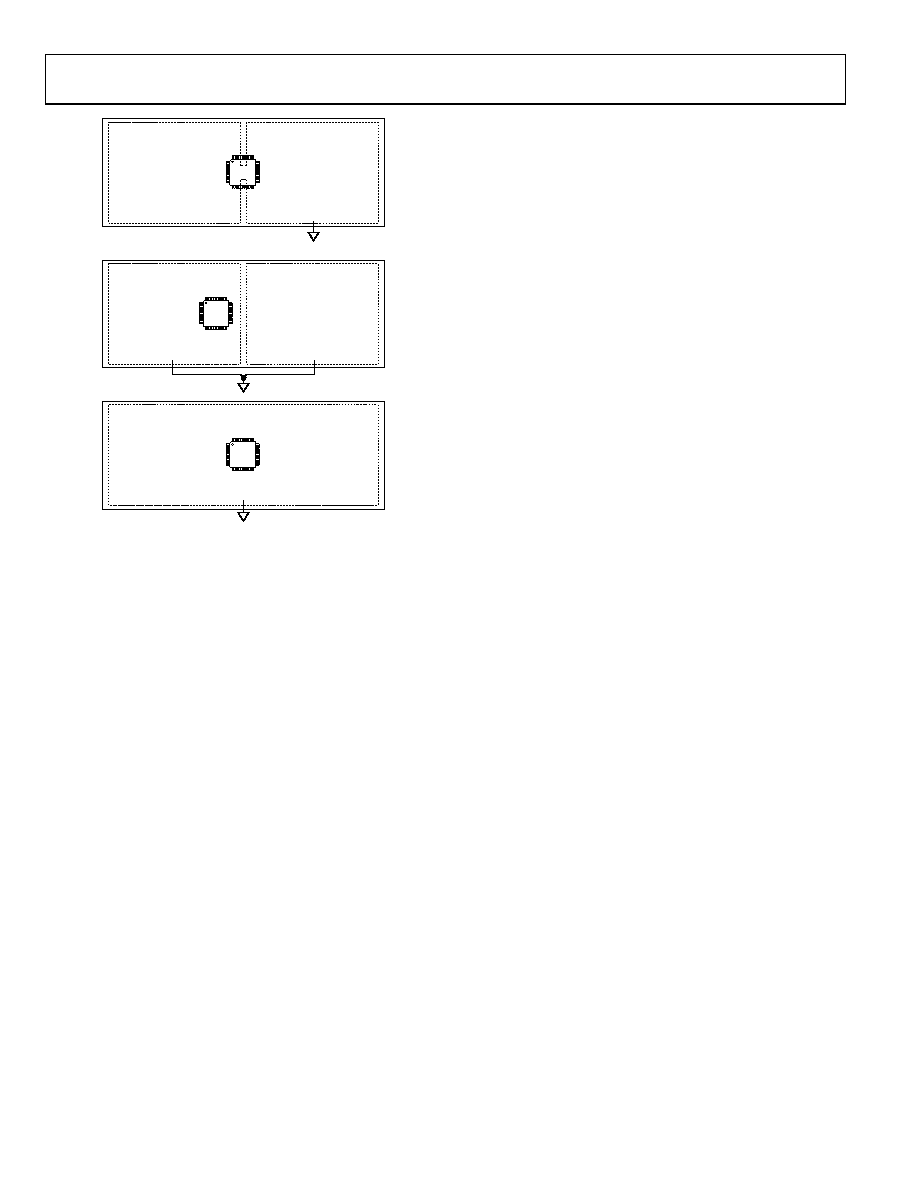
Figure 58. System Grounding Schemes
In all of these scenarios, and in more complicated real-life appli-
cations, keep in mind the flow of current from the supplies and
back to ground. Make sure the return paths for all currents are
as close as possible to the paths the currents took to reach their
destinations. For example, do not put power components on the
return currents from DVDD to flow through AGND. Also, try to
avoid digital currents flowing under analog circuitry, which
could happen if a noisy digital chip is placed on the left half of
the board in Figure 58c. Whenever possible, avoid large
discontinuities in the ground plane(s) (such as are formed by a
long trace on the same layer), because they force return signals
to travel a longer path. And of course, make all connections to
the ground plane directly, with little or no trace separating the
pin from its via to ground.
If the user plans to connect fast logic signals (rise/fall time
< 5 ns) to any of the ADuC814’s digital inputs, add a series
resistor to each relevant line to keep rise and fall times longer
than 5 ns at the ADuC814 input pins. A value of 100 or 200
is usually sufficient to prevent high speed signals from coupling
capacitively into the ADuC814 and affecting the accuracy of
ADC conversions.
OTHER HARDWARE CONSIDERATIONS
To facilitate in-circuit programming, in-circuit debug, and
emulation options, users should implement some simple
connection points in their hardware. A typical ADuC814
connection diagram is shown in Figure 59.
In-Circuit Serial Download Access
Nearly all ADuC814 designs will want to take advantage of the
in-circuit reprogrammability of the chip. This is accomplished
by a connection from the ADuC814’s UART to a PC, which
requires an external RS-232 chip for level translation. If users
would rather not design an RS-232 chip onto a board, refer to
the Application Note uC006, A 4-Wire UART-to-PC Interface
(available at www.analog.com/microconverter) for a simple
(and zero-cost-per-board) method of gaining in-circuit serial
download access to the ADuC814.
In addition to the basic UART connections, users also need a
way to trigger the chip into download mode. This is accom-
plished via a 1 k pull-up resistor that can be jumpered onto
the DLOAD pin. To get the ADuC814 into download mode,
simply connect this jumper and power-cycle the device (or
manually reset the device, if a manual reset button is available),
and it will be ready to receive a new program serially. To enable
the device to enter normal mode (and run the program) when-
ever power is cycled or RESET is toggled, the DLOAD pin must
be pulled low through a 1 k resistor.
Embedded Serial Port Debugger
From a hardware perspective, entry to serial port debug mode is
identical to the serial download entry sequence described in the
preceding section. In fact, both serial download and serial port
debug modes can be thought of as essentially one mode of
operation used in two different ways. Note that the serial port
debugger is fully contained on the ADuC814 device, unlike
ROM monitor type debuggers.
相关PDF资料 |
PDF描述 |
|---|---|
| AT32UC3C064C-ALUT | IC MCU AVR32 64K FLASH 144LQFP |
| VI-J1Z-IW-F4 | CONVERTER MOD DC/DC 2V 40W |
| ADUC7029BBCZ62I | IC MCU 12BIT 62KB FLASH 49BGA |
| VI-B2L-IY-F2 | CONVERTER MOD DC/DC 28V 50W |
| VJ2225A392KBAAT4X | CAP CER 3900PF 50V 10% NP0 2225 |
相关代理商/技术参数 |
参数描述 |
|---|---|
| ADUC814BRUZ-REEL | 功能描述:IC MCU 8K FLASH ADC/DAC 28-TSSOP RoHS:是 类别:集成电路 (IC) >> 嵌入式 - 微控制器, 系列:MicroConverter® ADuC8xx 标准包装:38 系列:Encore!® XP® 核心处理器:eZ8 芯体尺寸:8-位 速度:5MHz 连通性:IrDA,UART/USART 外围设备:欠压检测/复位,LED,POR,PWM,WDT 输入/输出数:16 程序存储器容量:4KB(4K x 8) 程序存储器类型:闪存 EEPROM 大小:- RAM 容量:1K x 8 电压 - 电源 (Vcc/Vdd):2.7 V ~ 3.6 V 数据转换器:- 振荡器型:内部 工作温度:-40°C ~ 105°C 封装/外壳:20-SOIC(0.295",7.50mm 宽) 包装:管件 其它名称:269-4116Z8F0413SH005EG-ND |
| ADUC814BRUZ-REEL7 | 功能描述:IC MCU 8K FLASH ADC/DAC 28-TSSOP RoHS:是 类别:集成电路 (IC) >> 嵌入式 - 微控制器, 系列:MicroConverter® ADuC8xx 标准包装:38 系列:Encore!® XP® 核心处理器:eZ8 芯体尺寸:8-位 速度:5MHz 连通性:IrDA,UART/USART 外围设备:欠压检测/复位,LED,POR,PWM,WDT 输入/输出数:16 程序存储器容量:4KB(4K x 8) 程序存储器类型:闪存 EEPROM 大小:- RAM 容量:1K x 8 电压 - 电源 (Vcc/Vdd):2.7 V ~ 3.6 V 数据转换器:- 振荡器型:内部 工作温度:-40°C ~ 105°C 封装/外壳:20-SOIC(0.295",7.50mm 宽) 包装:管件 其它名称:269-4116Z8F0413SH005EG-ND |
| ADUC816 | 制造商:未知厂家 制造商全称:未知厂家 功能描述:ADuC816: MicroConverter?= Dual 16-Bit ADC + 12-Bit DAC + Flash MCU Data Sheet (Rev. 0. 2/01 |
| ADUC816ASZ | 功能描述:8052 MicroConverter? ADuC8xx Microcontroller IC 8-Bit 12.58MHz 8KB (8K x 8) FLASH 制造商:analog devices inc. 系列:MicroConverter? ADuC8xx 包装:- 零件状态:上次购买时间 核心处理器:8052 核心尺寸:8-位 速度:12.58MHz 连接性:I2C,SPI,UART/USART 外设:PSM,温度传感器,WDT I/O 数:34 程序存储容量:8KB(8K x 8) 程序存储器类型:闪存 EEPROM 容量:640 x 8 RAM 容量:256 x 8 电压 - 电源(Vcc/Vdd):2.7 V ~ 5.5 V 数据转换器:A/D 7x16b;D/A 1x12b 振荡器类型:内部 工作温度:-40°C ~ 85°C(TA) 封装/外壳:- 供应商器件封装:- 标准包装:1 |
| ADUC816BCP | 功能描述:IC MCU 8K FLASH ADC/DAC 56LFCSP RoHS:否 类别:集成电路 (IC) >> 嵌入式 - 微控制器, 系列:MicroConverter® ADuC8xx 标准包装:38 系列:Encore!® XP® 核心处理器:eZ8 芯体尺寸:8-位 速度:5MHz 连通性:IrDA,UART/USART 外围设备:欠压检测/复位,LED,POR,PWM,WDT 输入/输出数:16 程序存储器容量:4KB(4K x 8) 程序存储器类型:闪存 EEPROM 大小:- RAM 容量:1K x 8 电压 - 电源 (Vcc/Vdd):2.7 V ~ 3.6 V 数据转换器:- 振荡器型:内部 工作温度:-40°C ~ 105°C 封装/外壳:20-SOIC(0.295",7.50mm 宽) 包装:管件 其它名称:269-4116Z8F0413SH005EG-ND |
发布紧急采购,3分钟左右您将得到回复。