- 您现在的位置:买卖IC网 > PDF目录11203 > ADUC843BCPZ8-3 (Analog Devices Inc)IC MCU FLASH 12BIT ADC 56LFCSP PDF资料下载
参数资料
| 型号: | ADUC843BCPZ8-3 |
| 厂商: | Analog Devices Inc |
| 文件页数: | 26/88页 |
| 文件大小: | 0K |
| 描述: | IC MCU FLASH 12BIT ADC 56LFCSP |
| 标准包装: | 1 |
| 系列: | MicroConverter® ADuC8xx |
| 核心处理器: | 8052 |
| 芯体尺寸: | 8-位 |
| 速度: | 8.38MHz |
| 连通性: | I²C,SPI,UART/USART |
| 外围设备: | DMA,PSM,PWM,温度传感器,WDT |
| 输入/输出数: | 32 |
| 程序存储器容量: | 8KB(8K x 8) |
| 程序存储器类型: | 闪存 |
| RAM 容量: | 2.25K x 8 |
| 电压 - 电源 (Vcc/Vdd): | 2.7 V ~ 3.6 V |
| 数据转换器: | A/D 8x12b |
| 振荡器型: | 内部 |
| 工作温度: | -40°C ~ 85°C |
| 封装/外壳: | 56-VFQFN 裸露焊盘,CSP |
| 包装: | 托盘 |
第1页第2页第3页第4页第5页第6页第7页第8页第9页第10页第11页第12页第13页第14页第15页第16页第17页第18页第19页第20页第21页第22页第23页第24页第25页当前第26页第27页第28页第29页第30页第31页第32页第33页第34页第35页第36页第37页第38页第39页第40页第41页第42页第43页第44页第45页第46页第47页第48页第49页第50页第51页第52页第53页第54页第55页第56页第57页第58页第59页第60页第61页第62页第63页第64页第65页第66页第67页第68页第69页第70页第71页第72页第73页第74页第75页第76页第77页第78页第79页第80页第81页第82页第83页第84页第85页第86页第87页第88页
ADuC841/ADuC842/ADuC843
Rev. 0 | Page 32 of 88
A 4 kByte Flash/EE data memory space is also provided on-
chip. This may be used as a general-purpose nonvolatile
scratchpad area. User access to this area is via a group of six
SFRs. This space can be programmed at a byte level, although it
must first be erased in 4-byte pages.
Flash/EE Memory Reliability
The Flash/EE program and data memory arrays on the parts are
fully qualified for two key Flash/EE memory characteristics:
Flash/EE memory cycling endurance and Flash/EE memory
data retention.
Endurance quantifies the ability of the Flash/EE memory to be
cycled through many program, read, and erase cycles. In real
terms, a single endurance cycle is composed of four independ-
ent, sequential events, defined as
1.
Initial page erase sequence.
2.
Read/verify sequence a single Flash/EE.
3.
Byte program sequence memory.
4.
Second read/verify sequence endurance cycle.
In reliability qualification, every byte in both the program and
data Flash/EE memory is cycled from 00H to FFH until a first
fail is recorded, signifying the endurance limit of the on-chip
Flash/EE memory.
As indicated in the Specifications table, the parts’ Flash/EE
memory endurance qualification has been carried out in
accordance with JEDEC Retention Lifetime Specification A117
over the industrial temperature range of –40°C to +25°C and
+25°C to +85°C. The results allow the specification of a mini-
mum endurance figure over supply and over temperature of
100,000 cycles, with an endurance figure of 700,000 cycles being
typical of operation at 25°C.
Retention quantifies the ability of the Flash/EE memory to
retain its programmed data over time. Again, the parts have
been qualified in accordance with the formal JEDEC Retention
Lifetime Specification (A117) at a specific junction temperature
(TJ = 55°C). As part of this qualification procedure, the Flash/EE
memory is cycled to its specified endurance limit, described
previously, before data retention is characterized. This means
that the Flash/EE memory is guaranteed to retain its data for its
fully specified retention lifetime every time the Flash/EE
memory is reprogrammed. Also note that retention lifetime,
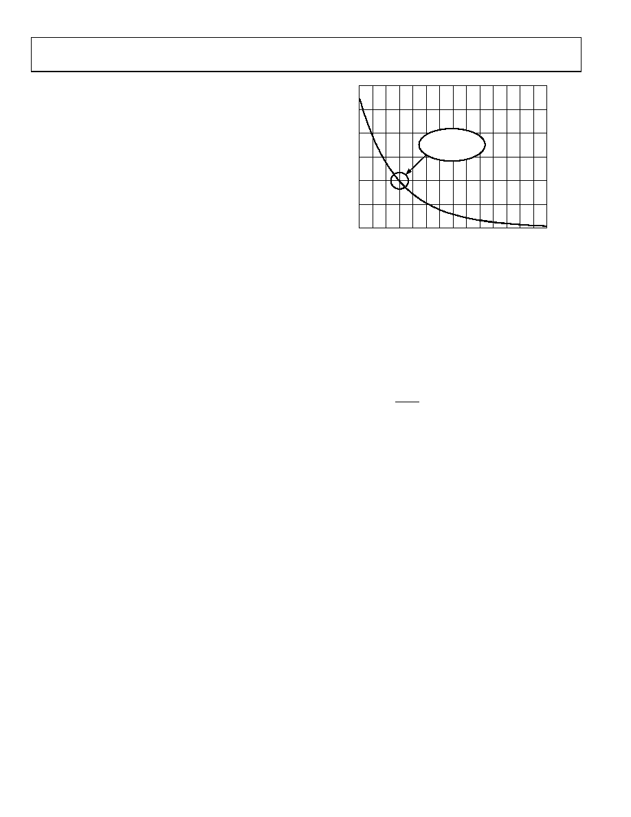
based on an activation energy of 0.6 eV, derates with TJ as
shown in Figure 38.
40
60
70
90
TJ JUNCTION TEMPERATURE (°C)
RE
TE
NTION
(Years)
250
200
150
100
50
0
50
80
110
300
100
ADI SPECIFICATION
100 YEARS MIN.
AT TJ = 55°C
03260-0-037
Figure 38. Flash/EE Memory Data Retention
Using the Flash/EE Program Memory
The 62 kByte Flash/EE program memory array is mapped into
the lower 62 kBytes of the 64 kByte program space addressable
by the parts, and is used to hold user code in typical applica-
tions. The program Flash/EE memory array can be
programmed in three ways:
Serial Downloading (In-Circuit Programming)
The parts facilitate code download via the standard UART serial
port. The parts enter serial download mode after a reset or
power cycle if the PSEN pin is pulled low through an external
1 k resistor. Once in serial download mode, the user can
download code to the full 62 kBytes of Flash/EE program
memory while the device is in-circuit in its target application
hardware.
A PC serial download executable is provided as part of the
ADuC841/ADuC842 QuickStart development system. The
serial download protocol is detailed in MicroConverter
Application Note uC004.
Parallel Programming
Parallel programming mode is fully compatible with conven-
tional third party flash or EEPROM device programmers. In
this mode, Ports P0, P1, and P2 operate as the external data and
address bus interface, ALE operates as the write enable strobe,
and Port P3 is used as a general configuration port, which
configures the device for various program and erase operations
during parallel programming. The high voltage (12 V) supply
required for flash programming is generated using on-chip
charge pumps to supply the high voltage program lines. The
complete parallel programming specification is available on the
MicroConverter home page at www.analog.com/microconverter.
相关PDF资料 |
PDF描述 |
|---|---|
| VI-BTF-IX | CONVERTER MOD DC/DC 72V 75W |
| ADUC843BCPZ8-5 | IC MCU FLASH 12BIT ADC 56LFCSP |
| VI-BTF-IW | CONVERTER MOD DC/DC 72V 100W |
| VI-BT4-IX | CONVERTER MOD DC/DC 48V 75W |
| ADUC7020BCPZ62-RL7 | IC MCU 12BIT 1MSPS UART 40-LFCSP |
相关代理商/技术参数 |
参数描述 |
|---|---|
| ADUC843BCPZ8-5 | 功能描述:IC MCU FLASH 12BIT ADC 56LFCSP RoHS:是 类别:集成电路 (IC) >> 嵌入式 - 微控制器, 系列:MicroConverter® ADuC8xx 标准包装:38 系列:Encore!® XP® 核心处理器:eZ8 芯体尺寸:8-位 速度:5MHz 连通性:IrDA,UART/USART 外围设备:欠压检测/复位,LED,POR,PWM,WDT 输入/输出数:16 程序存储器容量:4KB(4K x 8) 程序存储器类型:闪存 EEPROM 大小:- RAM 容量:1K x 8 电压 - 电源 (Vcc/Vdd):2.7 V ~ 3.6 V 数据转换器:- 振荡器型:内部 工作温度:-40°C ~ 105°C 封装/外壳:20-SOIC(0.295",7.50mm 宽) 包装:管件 其它名称:269-4116Z8F0413SH005EG-ND |
| ADUC843BS62-3 | 制造商:Analog Devices 功能描述:MCU 8-Bit ADuC8xx 8052 CISC 62KB Flash 3V 52-Pin MQFP |
| ADUC843BS62-5 | 制造商:Analog Devices 功能描述:IC MICROCONTROLLER |
| ADUC843BSZ62-3 | 功能描述:IC ADC 12BIT W/FLASH MCU 52-MQFP RoHS:是 类别:集成电路 (IC) >> 嵌入式 - 微控制器, 系列:MicroConverter® ADuC8xx 标准包装:250 系列:LPC11Uxx 核心处理器:ARM? Cortex?-M0 芯体尺寸:32-位 速度:50MHz 连通性:I²C,Microwire,SPI,SSI,SSP,UART/USART,USB 外围设备:欠压检测/复位,POR,WDT 输入/输出数:40 程序存储器容量:96KB(96K x 8) 程序存储器类型:闪存 EEPROM 大小:4K x 8 RAM 容量:10K x 8 电压 - 电源 (Vcc/Vdd):1.8 V ~ 3.6 V 数据转换器:A/D 8x10b 振荡器型:内部 工作温度:-40°C ~ 85°C 封装/外壳:48-LQFP 包装:托盘 其它名称:568-9587 |
| ADUC843BSZ62-5 | 功能描述:IC ADC 12BIT W/FLASH MCU 52-MQFP RoHS:是 类别:集成电路 (IC) >> 嵌入式 - 微控制器, 系列:MicroConverter® ADuC8xx 标准包装:60 系列:PSOC® 3 CY8C38xx 核心处理器:8051 芯体尺寸:8-位 速度:67MHz 连通性:EBI/EMI,I²C,LIN,SPI,UART/USART 外围设备:电容感应,DMA,LCD,POR,PWM,WDT 输入/输出数:25 程序存储器容量:64KB(64K x 8) 程序存储器类型:闪存 EEPROM 大小:2K x 8 RAM 容量:8K x 8 电压 - 电源 (Vcc/Vdd):1.71 V ~ 5.5 V 数据转换器:A/D 2x20b,D/A 4x8b 振荡器型:内部 工作温度:-40°C ~ 85°C 封装/外壳:48-VFQFN 裸露焊盘 包装:托盘 |
发布紧急采购,3分钟左右您将得到回复。