- 您现在的位置:买卖IC网 > PDF目录11203 > ADUC843BCPZ8-3 (Analog Devices Inc)IC MCU FLASH 12BIT ADC 56LFCSP PDF资料下载
参数资料
| 型号: | ADUC843BCPZ8-3 |
| 厂商: | Analog Devices Inc |
| 文件页数: | 55/88页 |
| 文件大小: | 0K |
| 描述: | IC MCU FLASH 12BIT ADC 56LFCSP |
| 标准包装: | 1 |
| 系列: | MicroConverter® ADuC8xx |
| 核心处理器: | 8052 |
| 芯体尺寸: | 8-位 |
| 速度: | 8.38MHz |
| 连通性: | I²C,SPI,UART/USART |
| 外围设备: | DMA,PSM,PWM,温度传感器,WDT |
| 输入/输出数: | 32 |
| 程序存储器容量: | 8KB(8K x 8) |
| 程序存储器类型: | 闪存 |
| RAM 容量: | 2.25K x 8 |
| 电压 - 电源 (Vcc/Vdd): | 2.7 V ~ 3.6 V |
| 数据转换器: | A/D 8x12b |
| 振荡器型: | 内部 |
| 工作温度: | -40°C ~ 85°C |
| 封装/外壳: | 56-VFQFN 裸露焊盘,CSP |
| 包装: | 托盘 |
第1页第2页第3页第4页第5页第6页第7页第8页第9页第10页第11页第12页第13页第14页第15页第16页第17页第18页第19页第20页第21页第22页第23页第24页第25页第26页第27页第28页第29页第30页第31页第32页第33页第34页第35页第36页第37页第38页第39页第40页第41页第42页第43页第44页第45页第46页第47页第48页第49页第50页第51页第52页第53页第54页当前第55页第56页第57页第58页第59页第60页第61页第62页第63页第64页第65页第66页第67页第68页第69页第70页第71页第72页第73页第74页第75页第76页第77页第78页第79页第80页第81页第82页第83页第84页第85页第86页第87页第88页
ADuC841/ADuC842/ADuC843
Rev. 0 | Page 59 of 88
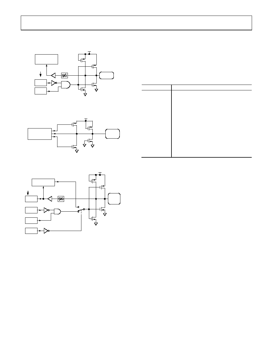
MOSI is shared with P3.3 and, as such, has the same
configuration as the one shown in Figure 61.
MCO
I2C M
Q3
Q4
SCLOCK
PIN
Q2
Q1
(OFF)
DVDD
50ns GLITCH
REJECTION FILTER
SPE = 0 (I2C ENABLE)
HARDWARE I2C
(SLAVE ONLY)
SFR
BITS
03260-0-062
Figure 63. SCLOCK Pin I/O Functional Equivalent in I2C Mode
Q3
Q1
Q2 (OFF)
DVDD
Q4 (OFF)
SDATA/
MOSI
PIN
SPE = 1 (SPI ENABLE)
HARDWARE SPI
(MASTER/SLAVE)
03260-0-097
Figure 64. SDATA/MOSI Pin I/O Functional Equivalent in SPI Mode
Q3
Q4
Q2
Q1
DVDD
MCO
SDATA/
MOSI
PIN
(OFF)
50ns GLITCH
REJECTION FILTER
SPE = 0 (I2C ENABLE)
HARDWARE I2C
(SLAVE ONLY)
SFR
BITS
MCI
MDE
I2C M
03260-0-063
Figure 65. SDATA/MOSI Pin I/O Functional Equivalent in I2C Mode
Read-Modify-Write Instructions
Some 8051 instructions that read a port read the latch while
others read the pin. The instructions that read the latch rather
than the pins are the ones that read a value, possibly change it,
and then rewrite it to the latch. These are called read-modify-
write instructions, which are listed below. When the destination
operand is a port or a port bit, these instructions read the latch
rather than the pin.
Table 27. Read-Write-Modify Instructions
Instruction
Description
ANL
Logical AND, e.g., ANL P1, A
ORL
(Logical OR, e.g., ORL P2, A
XRL
(Logical EX-OR, e.g., XRL P3, A
JBC
Jump if Bit = 1 and clear bit, e.g., JBC P1.1,
LABEL
CPL
Complement bit, e.g., CPL P3.0
INC
Increment, e.g., INC P2
DEC
Decrement, e.g., DEC P2
DJNZ
Decrement and Jump if Not Zero, e.g., DJNZ
P3, LABEL
MOV PX.Y, C1
Move Carry to Bit Y of Port X
CLR PX.Y1
Clear Bit Y of Port X
SETB PX.Y1
Set Bit Y of Port X
1 These instructions read the port byte (all 8 bits), modify the addressed bit,
and then write the new byte back to the latch.
Read-modify-write instructions are directed to the latch rather
than to the pin to avoid a possible misinterpretation of the
voltage level of a pin. For example, a port pin might be used to
drive the base of a transistor. When 1 is written to the bit, the
transistor is turned on. If the CPU then reads the same port bit
at the pin rather than the latch, it reads the base voltage of the
transistor and interprets it as a Logic 0. Reading the latch rather
than the pin returns the correct value of 1.
相关PDF资料 |
PDF描述 |
|---|---|
| VI-BTF-IX | CONVERTER MOD DC/DC 72V 75W |
| ADUC843BCPZ8-5 | IC MCU FLASH 12BIT ADC 56LFCSP |
| VI-BTF-IW | CONVERTER MOD DC/DC 72V 100W |
| VI-BT4-IX | CONVERTER MOD DC/DC 48V 75W |
| ADUC7020BCPZ62-RL7 | IC MCU 12BIT 1MSPS UART 40-LFCSP |
相关代理商/技术参数 |
参数描述 |
|---|---|
| ADUC843BCPZ8-5 | 功能描述:IC MCU FLASH 12BIT ADC 56LFCSP RoHS:是 类别:集成电路 (IC) >> 嵌入式 - 微控制器, 系列:MicroConverter® ADuC8xx 标准包装:38 系列:Encore!® XP® 核心处理器:eZ8 芯体尺寸:8-位 速度:5MHz 连通性:IrDA,UART/USART 外围设备:欠压检测/复位,LED,POR,PWM,WDT 输入/输出数:16 程序存储器容量:4KB(4K x 8) 程序存储器类型:闪存 EEPROM 大小:- RAM 容量:1K x 8 电压 - 电源 (Vcc/Vdd):2.7 V ~ 3.6 V 数据转换器:- 振荡器型:内部 工作温度:-40°C ~ 105°C 封装/外壳:20-SOIC(0.295",7.50mm 宽) 包装:管件 其它名称:269-4116Z8F0413SH005EG-ND |
| ADUC843BS62-3 | 制造商:Analog Devices 功能描述:MCU 8-Bit ADuC8xx 8052 CISC 62KB Flash 3V 52-Pin MQFP |
| ADUC843BS62-5 | 制造商:Analog Devices 功能描述:IC MICROCONTROLLER |
| ADUC843BSZ62-3 | 功能描述:IC ADC 12BIT W/FLASH MCU 52-MQFP RoHS:是 类别:集成电路 (IC) >> 嵌入式 - 微控制器, 系列:MicroConverter® ADuC8xx 标准包装:250 系列:LPC11Uxx 核心处理器:ARM? Cortex?-M0 芯体尺寸:32-位 速度:50MHz 连通性:I²C,Microwire,SPI,SSI,SSP,UART/USART,USB 外围设备:欠压检测/复位,POR,WDT 输入/输出数:40 程序存储器容量:96KB(96K x 8) 程序存储器类型:闪存 EEPROM 大小:4K x 8 RAM 容量:10K x 8 电压 - 电源 (Vcc/Vdd):1.8 V ~ 3.6 V 数据转换器:A/D 8x10b 振荡器型:内部 工作温度:-40°C ~ 85°C 封装/外壳:48-LQFP 包装:托盘 其它名称:568-9587 |
| ADUC843BSZ62-5 | 功能描述:IC ADC 12BIT W/FLASH MCU 52-MQFP RoHS:是 类别:集成电路 (IC) >> 嵌入式 - 微控制器, 系列:MicroConverter® ADuC8xx 标准包装:60 系列:PSOC® 3 CY8C38xx 核心处理器:8051 芯体尺寸:8-位 速度:67MHz 连通性:EBI/EMI,I²C,LIN,SPI,UART/USART 外围设备:电容感应,DMA,LCD,POR,PWM,WDT 输入/输出数:25 程序存储器容量:64KB(64K x 8) 程序存储器类型:闪存 EEPROM 大小:2K x 8 RAM 容量:8K x 8 电压 - 电源 (Vcc/Vdd):1.71 V ~ 5.5 V 数据转换器:A/D 2x20b,D/A 4x8b 振荡器型:内部 工作温度:-40°C ~ 85°C 封装/外壳:48-VFQFN 裸露焊盘 包装:托盘 |
发布紧急采购,3分钟左右您将得到回复。