- 您现在的位置:买卖IC网 > PDF目录11201 > ADUC847BSZ8-3 (Analog Devices Inc)IC MCU FLASH W/24BIT ADC 52MQFP PDF资料下载
参数资料
| 型号: | ADUC847BSZ8-3 |
| 厂商: | Analog Devices Inc |
| 文件页数: | 12/108页 |
| 文件大小: | 0K |
| 描述: | IC MCU FLASH W/24BIT ADC 52MQFP |
| 标准包装: | 1 |
| 系列: | MicroConverter® ADuC8xx |
| 核心处理器: | 8052 |
| 芯体尺寸: | 8-位 |
| 速度: | 12.58MHz |
| 连通性: | I²C,SPI,UART/USART |
| 外围设备: | POR,PSM,PWM,温度传感器,WDT |
| 输入/输出数: | 34 |
| 程序存储器容量: | 8KB(8K x 8) |
| 程序存储器类型: | 闪存 |
| EEPROM 大小: | 4K x 8 |
| RAM 容量: | 2.25K x 8 |
| 电压 - 电源 (Vcc/Vdd): | 2.7 V ~ 3.6 V |
| 数据转换器: | A/D 10x24b; D/A 1x12b,2x16b |
| 振荡器型: | 内部 |
| 工作温度: | -40°C ~ 125°C |
| 封装/外壳: | 52-QFP |
| 包装: | 托盘 |
| 配用: | EVAL-ADUC847QSZ-ND - KIT DEV QUICK START FOR ADUC847 |
第1页第2页第3页第4页第5页第6页第7页第8页第9页第10页第11页当前第12页第13页第14页第15页第16页第17页第18页第19页第20页第21页第22页第23页第24页第25页第26页第27页第28页第29页第30页第31页第32页第33页第34页第35页第36页第37页第38页第39页第40页第41页第42页第43页第44页第45页第46页第47页第48页第49页第50页第51页第52页第53页第54页第55页第56页第57页第58页第59页第60页第61页第62页第63页第64页第65页第66页第67页第68页第69页第70页第71页第72页第73页第74页第75页第76页第77页第78页第79页第80页第81页第82页第83页第84页第85页第86页第87页第88页第89页第90页第91页第92页第93页第94页第95页第96页第97页第98页第99页第100页第101页第102页第103页第104页第105页第106页第107页第108页
Data Sheet
ADuC845/ADuC847/ADuC848
Rev. C | Page 11 of 108
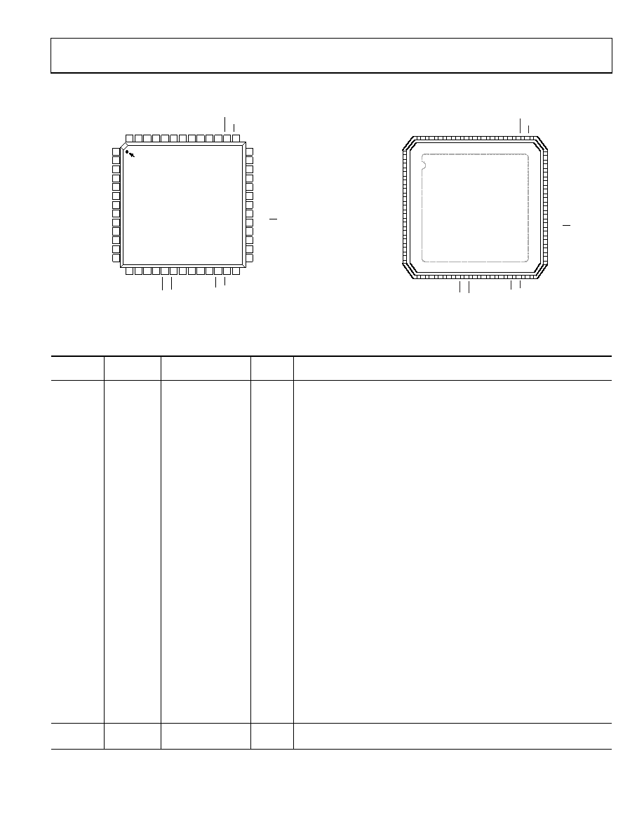
PIN CONFIGURATIONS AND FUNCTION DESCRIPTIONS
52 51 50 49 48
43 42 41 40
47 46 45 44
14 15 16 17 18 19 20 21 22 23 24 25 26
1
2
3
4
5
6
7
8
9
10
11
13
12
PIN 1
IDENTIFIER
TOP VIEW
(Not to Scale)
39
38
37
36
35
34
33
32
31
30
29
28
27
P0.7/AD7
P0.6/AD6
P0.5/AD5
P0.4/AD4
DV
DD
DGND
P0.3/AD3
P0.2/AD2
P0.1/AD1
P0.0/AD0
ALE
PSEN
EA
DAC
RESET
P3.0/RxD
P3.1/TxD
P3.2/INT0
P3.3/INT1
DV
DD
P3.4/T0
P3.5/T1
P3.6/WR
P3.7/RD
SCLOCK
(I
2
C)
P1.0/AIN1
P1.1/AIN2
P1.2/AIN3/REFIN2+
P1.3/AIN4/REFIN2–
AVDD
AGND
REFIN–
REFIN+
P1.4/AIN5
P1.5/AIN6
P1.6/AIN7/IEXC1
P1.7/AIN8/IEXC2
AINCOM/DAC
P2.7/PWMCLK
P2.6/PWM1
P2.5/PWM0
P2.4/T2EX
DGND
DVDD
XTAL2
XTAL1
P2.3/SS/T2
P2.2/MISO
P2.1/MOSI
P2.0/SCLOCK (SPI)
SDATA
DGND
04741-002
ADuC845/ADuC847/ADuC848
Figure 2. 52-Lead MQFP Pin Configuration
04741-
003
P1.1/AIN2
P1.2/AIN3/REFIN2+
P1.3/AIN4/REFIN2–
AGND
AVDD
AGND
REFIN–
REFIN+
P1.4/AIN5
P1.5/AIN6
P1.6/AIN7/IEXC1
P1.7/AIN8/IEXC2
AINCOM/DAC
DAC
AI
N9
AI
N10
R
ESET
P
3.
0/
RxD
P
3.
1/
T
xD
P
3
.2
/IN
T0
P
3
.3
/IN
T1
DV
DD
DG
ND
P
3
.4
/T0
P
3
.5
/T1
P
3.
6/
W
R
P
3.
7/
RD
S
CL
K
(
I2
C)
P2.7/PWMCLK
P2.6/PWM1
P2.5/PWM0
P2.4/T2EX
DGND
DVDD
XTAL1
P2.3/SS/T2
P2.2/MISO
P2.1/MOSI
P2.0/SCLOCK (SPI)
SDATA
P
1.
0/
AI
N1
P
0.
7/
AD7
P
0.
6/
AD6
P
0.
5/
AD5
P
0.
4/
AD4
DV
DD
DG
ND
P
0.
3/
AD3
P
0.
2/
AD2
P
0.
1/
AD1
P
0.
0/
AD0
AL
E
PSEN
EA
14
1
2
3
4
5
6
7
8
9
10
11
13
12
15
16
17
18
19
20
21
22
23
24
25
26
27
28
42
41
40
39
38
37
36
35
34
33
32
31
30
29
43
45
46
47
48
49
50
51
52
53
54
55
56
44
XTAL2
TOP VIEW
(Not to Scale)
ADuC845/ADuC847/
ADuC848
NOTES
1. THE EXPOSED PADDLE MUST BE LEFT UNCONNECTED.
Figure 3. 56-Lead LFCSP Pin Configuration
Table 3. Pin Function Descriptions
Pin No:
52-MQFP
Pin No:
56-LFCSP
Mnemonic
Type1
Description
1
56
P1.0/AIN1
I
By power-on default, P1.0/AIN1 is configured as the AIN1 analog input.
AIN1 can be used as a pseudo differential input when used with AINCOM or as
the positive input of a fully differential pair when used with AIN2.
P1.0 has no digital output driver. It can function as a digital input for which 0
must be written to the port bit. As a digital input, this pin must be driven high
or low externally.
2
1
P1.1/AIN2
I
On power-on default, P1.1/AIN2 is configured as the AIN2 analog input.
AIN2 can be used as a pseudo differential input when used with AINCOM or as
the negative input of a fully differential pair when used with AIN1.
P1.1 has no digital output driver. It can function as a digital input for which 0
must be written to the port bit. As a digital input, this pin must be driven high
or low externally.
3
2
P1.2/AIN3/REFIN2+
I
On power-on default, P1.2/AIN3 is configured as the AIN3 analog input.
AIN3 can be used as a pseudo differential input when used with AINCOM or as
the positive input of a fully differential pair when used with AIN4.
P1.2 has no digital output driver. It can function as a digital input for which 0
must be written to the port bit. As a digital input, this pin must be driven high
or low externally. This pin also functions as a second external differential
reference input, positive terminal.
4
3
P1.3/AIN4/REFIN2
I
On power-on default, P1.3/AIN4 is configured as the AIN4 analog input.
AIN4 can be used as a pseudo differential input when used with AINCOM or as
the negative input of a fully differential pair when used with AIN3.
P1.3 has no digital output driver. It can function as a digital input for which 0
must be written to the port bit. As a digital input, this pin must be driven high
or low externally. This pin also functions as a second external differential
reference input, negative terminal.
5
4
AVDD
S
Analog Supply Voltage.
6
5
AGND
S
Analog Ground.
---
6
AGND
S
A second analog ground is provided with the LFCSP version only.
7
REFIN
I
External Differential Reference Input, Negative Terminal.
8
REFIN+
I
External Differential Reference Input, Positive Terminal.
Footnotes at end of table.
相关PDF资料 |
PDF描述 |
|---|---|
| VE-B4T-IW | CONVERTER MOD DC/DC 6.5V 100W |
| AT91SAM9261B-CU-999 | IC MCU ARM9 ULT LOW PWR 217LFBGA |
| VE-B4R-IX | CONVERTER MOD DC/DC 7.5V 75W |
| ATMEGA128-16MUR | MCU AVR 128KB FLASH 16MHZ 64QFN |
| VE-B4R-IW | CONVERTER MOD DC/DC 7.5V 100W |
相关代理商/技术参数 |
参数描述 |
|---|---|
| ADUC847BSZ8-5 | 功能描述:IC MCU FLASH W/24BIT ADC 52MQFP RoHS:是 类别:集成电路 (IC) >> 嵌入式 - 微控制器, 系列:MicroConverter® ADuC8xx 标准包装:38 系列:Encore!® XP® 核心处理器:eZ8 芯体尺寸:8-位 速度:5MHz 连通性:IrDA,UART/USART 外围设备:欠压检测/复位,LED,POR,PWM,WDT 输入/输出数:16 程序存储器容量:4KB(4K x 8) 程序存储器类型:闪存 EEPROM 大小:- RAM 容量:1K x 8 电压 - 电源 (Vcc/Vdd):2.7 V ~ 3.6 V 数据转换器:- 振荡器型:内部 工作温度:-40°C ~ 105°C 封装/外壳:20-SOIC(0.295",7.50mm 宽) 包装:管件 其它名称:269-4116Z8F0413SH005EG-ND |
| ADUC848 | 制造商:AD 制造商全称:Analog Devices 功能描述:MicroConverter Multichannel 24-/16-Bit ADCs with Embedded 62 kB Flash and Single-Cycle MCU |
| ADUC848BCP32-3 | 制造商:Analog Devices 功能描述:10 CHANNEL 16 BIT ADC + FLASH 8 BIT UP - Trays |
| ADUC848BCP32-5 | 制造商:Analog Devices 功能描述:10 CHANNEL 16 BIT ADC + FLASH 8 BIT UP - Trays |
| ADUC848BCP62-3 | 制造商:Analog Devices 功能描述:MCU 8-Bit ADuC8xx 8052 CISC 62KB Flash 3.3V/5V 56-Pin LFCSP EP 制造商:Rochester Electronics LLC 功能描述:8BIT CISC 62KB FLASH 12.85MHZ 3.3V 56LFCSP - Bulk |
发布紧急采购,3分钟左右您将得到回复。