- 您现在的位置:买卖IC网 > PDF目录11201 > ADUC847BSZ8-3 (Analog Devices Inc)IC MCU FLASH W/24BIT ADC 52MQFP PDF资料下载
参数资料
| 型号: | ADUC847BSZ8-3 |
| 厂商: | Analog Devices Inc |
| 文件页数: | 81/108页 |
| 文件大小: | 0K |
| 描述: | IC MCU FLASH W/24BIT ADC 52MQFP |
| 标准包装: | 1 |
| 系列: | MicroConverter® ADuC8xx |
| 核心处理器: | 8052 |
| 芯体尺寸: | 8-位 |
| 速度: | 12.58MHz |
| 连通性: | I²C,SPI,UART/USART |
| 外围设备: | POR,PSM,PWM,温度传感器,WDT |
| 输入/输出数: | 34 |
| 程序存储器容量: | 8KB(8K x 8) |
| 程序存储器类型: | 闪存 |
| EEPROM 大小: | 4K x 8 |
| RAM 容量: | 2.25K x 8 |
| 电压 - 电源 (Vcc/Vdd): | 2.7 V ~ 3.6 V |
| 数据转换器: | A/D 10x24b; D/A 1x12b,2x16b |
| 振荡器型: | 内部 |
| 工作温度: | -40°C ~ 125°C |
| 封装/外壳: | 52-QFP |
| 包装: | 托盘 |
| 配用: | EVAL-ADUC847QSZ-ND - KIT DEV QUICK START FOR ADUC847 |
第1页第2页第3页第4页第5页第6页第7页第8页第9页第10页第11页第12页第13页第14页第15页第16页第17页第18页第19页第20页第21页第22页第23页第24页第25页第26页第27页第28页第29页第30页第31页第32页第33页第34页第35页第36页第37页第38页第39页第40页第41页第42页第43页第44页第45页第46页第47页第48页第49页第50页第51页第52页第53页第54页第55页第56页第57页第58页第59页第60页第61页第62页第63页第64页第65页第66页第67页第68页第69页第70页第71页第72页第73页第74页第75页第76页第77页第78页第79页第80页当前第81页第82页第83页第84页第85页第86页第87页第88页第89页第90页第91页第92页第93页第94页第95页第96页第97页第98页第99页第100页第101页第102页第103页第104页第105页第106页第107页第108页
ADuC845/ADuC847/ADuC848
Data Sheet
Rev. C | Page 74 of 108
P2.5 and P2.6 can also be used as PWM outputs, while P2.7 can
act as an alternate PWM clock source. When selected as the
PWM outputs, they overwrite anything written to P2.5 or P2.6.
Table 47. Port 2 Alternate Functions
Pin No.
Alternate Function
P2.0
SCLOCK for SPI
P2.1
MOSI for SPI
P2.2
MISO for SPI
P2.3
SS and T2 clock input
P2.4
T2EX alternate control for T2
P2.5
PWM0 output
P2.6
PWM1 output
P2.7
PWMCLK
CONTROL
READ
LATCH
INTERNAL
BUS
WRITE
TO LATCH
READ
PIN
D
CL
Q
LATCH
DVDD
ADDR
P2.x
PIN
DVDD
INTERNAL
PULL-UP
Q
04741-069
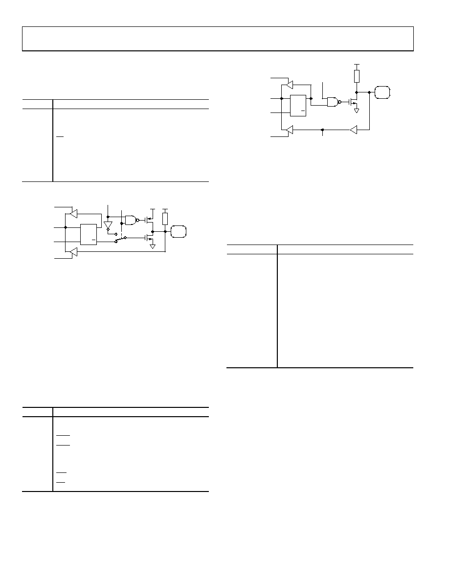
Figure 50. Port 2 Bit Latch and I/O Buffer
Port 3
Port 3 is a bidirectional port with internal pull-ups directly
controlled via the P3 SFR (B0H). Port 3 pins that have 1s
written to them are pulled high by the internal pull-ups and, in
that state, can be used as inputs. As inputs, Port 3 pins pulled
externally low source current because of the internal pull-ups.
Port 3 pins with 0s written to them drive a logic low output
voltage (VOL) and are capable of sinking 4 mA. Port 3 pins also
have various secondary functions as described in Table 48. The
alternate functions of Port 3 pins can be activated only if the
corresponding bit latch in the P3 SFR contains a 1. Otherwise,
the port pin remains at 0.
Table 48. Port 3 Alternate Functions
Pin No.
Alternate Function
P3.0
RxD (UART input pin, or serial data I/O in Mode 0)
P3.1
TxD (UART output pin, or serial clock output in Mode 0)
P3.2
INT0 (External Interrupt 0)
P3.3
INT1 (External Interrupt 1)
P3.4
T0 (Timer/Counter 0 external input)
P3.5
T1 (Timer/Counter 1 external input)
P3.6
WR (external data memory write strobe)
P3.7
RD (external data memory read strobe)
READ
LATCH
INTERNAL
BUS
WRITE
TO LATCH
READ
PIN
D
CL
Q
LATCH
DVDD
P3.x
PIN
INTERNAL
PULL-UP
ALTERNATE
OUTPUT
FUNCTION
ALTERNATE
INPUT
FUNCTION
Q
04741-071
Figure 51. Port 3 Bit Latch and I/O Buffer
Read-Modify-Write Instructions
Some 8051 instructions read the latch while others read the pin.
The instructions that read the latch rather than the pins are the
ones that read a value, possibly change it, and rewrite it to the
latch. These are called read-modify-write instructions, which
are listed in Table 49. When the destination operand is a port or
a port bit, these instructions read the latch rather than the pin.
Table 49. Read-Modify-Write Instructions
Instruction
Description
ANL
Logical AND, for example, ANL P1, A
ORL
Logical OR, for example, ORL P2, A
XRL
Logical EX-OR, for example, XRL P3, A
JBC
Jump if Bit = 1 and clear bit, for example, JBC
P1.1, LABEL
CPL
Complement bit, for example, CPL P3.0
INC
Increment, for example, INC P2
DEC
Decrement, for example, DEC P2
DJNZ
Decrement and jump if not zero, for example,
DJNZ P3, LABEL
MOV PX.Y, C1
Move Carry to Bit Y of Port X
CLR PX.Y1
Clear Bit Y of Port X
SETB PX.Y1
Set Bit Y of Port X
___________________________________________
1
These instructions read the port byte (all 8 bits), modify the addressed bit,
and write the new byte back to the latch.
Read-modify-write instructions are directed to the latch rather
than to the pin to avoid a possible misinterpretation of the
voltage level of a pin. For example, a port pin might be used to
drive the base of a transistor. When 1 is written to the bit, the
transistor is turned on. If the CPU reads the same port bit at the
pin rather than the latch, it reads the base voltage of the
transistor and interprets it as Logic 0. Reading the latch rather
than the pin returns the correct value of 1.
相关PDF资料 |
PDF描述 |
|---|---|
| VE-B4T-IW | CONVERTER MOD DC/DC 6.5V 100W |
| AT91SAM9261B-CU-999 | IC MCU ARM9 ULT LOW PWR 217LFBGA |
| VE-B4R-IX | CONVERTER MOD DC/DC 7.5V 75W |
| ATMEGA128-16MUR | MCU AVR 128KB FLASH 16MHZ 64QFN |
| VE-B4R-IW | CONVERTER MOD DC/DC 7.5V 100W |
相关代理商/技术参数 |
参数描述 |
|---|---|
| ADUC847BSZ8-5 | 功能描述:IC MCU FLASH W/24BIT ADC 52MQFP RoHS:是 类别:集成电路 (IC) >> 嵌入式 - 微控制器, 系列:MicroConverter® ADuC8xx 标准包装:38 系列:Encore!® XP® 核心处理器:eZ8 芯体尺寸:8-位 速度:5MHz 连通性:IrDA,UART/USART 外围设备:欠压检测/复位,LED,POR,PWM,WDT 输入/输出数:16 程序存储器容量:4KB(4K x 8) 程序存储器类型:闪存 EEPROM 大小:- RAM 容量:1K x 8 电压 - 电源 (Vcc/Vdd):2.7 V ~ 3.6 V 数据转换器:- 振荡器型:内部 工作温度:-40°C ~ 105°C 封装/外壳:20-SOIC(0.295",7.50mm 宽) 包装:管件 其它名称:269-4116Z8F0413SH005EG-ND |
| ADUC848 | 制造商:AD 制造商全称:Analog Devices 功能描述:MicroConverter Multichannel 24-/16-Bit ADCs with Embedded 62 kB Flash and Single-Cycle MCU |
| ADUC848BCP32-3 | 制造商:Analog Devices 功能描述:10 CHANNEL 16 BIT ADC + FLASH 8 BIT UP - Trays |
| ADUC848BCP32-5 | 制造商:Analog Devices 功能描述:10 CHANNEL 16 BIT ADC + FLASH 8 BIT UP - Trays |
| ADUC848BCP62-3 | 制造商:Analog Devices 功能描述:MCU 8-Bit ADuC8xx 8052 CISC 62KB Flash 3.3V/5V 56-Pin LFCSP EP 制造商:Rochester Electronics LLC 功能描述:8BIT CISC 62KB FLASH 12.85MHZ 3.3V 56LFCSP - Bulk |
发布紧急采购,3分钟左右您将得到回复。