- 您现在的位置:买卖IC网 > PDF目录11201 > ADUC847BSZ8-3 (Analog Devices Inc)IC MCU FLASH W/24BIT ADC 52MQFP PDF资料下载
参数资料
| 型号: | ADUC847BSZ8-3 |
| 厂商: | Analog Devices Inc |
| 文件页数: | 60/108页 |
| 文件大小: | 0K |
| 描述: | IC MCU FLASH W/24BIT ADC 52MQFP |
| 标准包装: | 1 |
| 系列: | MicroConverter® ADuC8xx |
| 核心处理器: | 8052 |
| 芯体尺寸: | 8-位 |
| 速度: | 12.58MHz |
| 连通性: | I²C,SPI,UART/USART |
| 外围设备: | POR,PSM,PWM,温度传感器,WDT |
| 输入/输出数: | 34 |
| 程序存储器容量: | 8KB(8K x 8) |
| 程序存储器类型: | 闪存 |
| EEPROM 大小: | 4K x 8 |
| RAM 容量: | 2.25K x 8 |
| 电压 - 电源 (Vcc/Vdd): | 2.7 V ~ 3.6 V |
| 数据转换器: | A/D 10x24b; D/A 1x12b,2x16b |
| 振荡器型: | 内部 |
| 工作温度: | -40°C ~ 125°C |
| 封装/外壳: | 52-QFP |
| 包装: | 托盘 |
| 配用: | EVAL-ADUC847QSZ-ND - KIT DEV QUICK START FOR ADUC847 |
第1页第2页第3页第4页第5页第6页第7页第8页第9页第10页第11页第12页第13页第14页第15页第16页第17页第18页第19页第20页第21页第22页第23页第24页第25页第26页第27页第28页第29页第30页第31页第32页第33页第34页第35页第36页第37页第38页第39页第40页第41页第42页第43页第44页第45页第46页第47页第48页第49页第50页第51页第52页第53页第54页第55页第56页第57页第58页第59页当前第60页第61页第62页第63页第64页第65页第66页第67页第68页第69页第70页第71页第72页第73页第74页第75页第76页第77页第78页第79页第80页第81页第82页第83页第84页第85页第86页第87页第88页第89页第90页第91页第92页第93页第94页第95页第96页第97页第98页第99页第100页第101页第102页第103页第104页第105页第106页第107页第108页
Data Sheet
ADuC845/ADuC847/ADuC848
Rev. C | Page 55 of 108
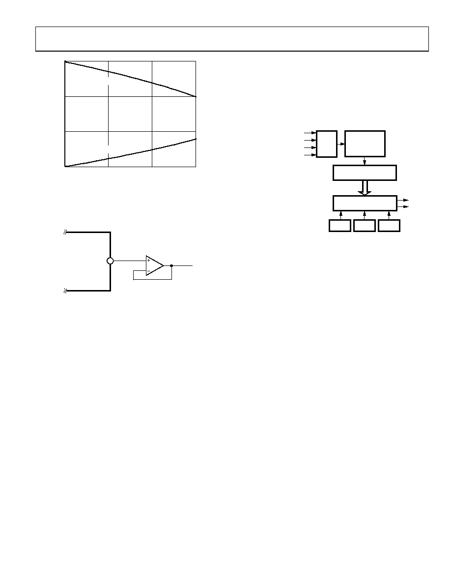
SOURCE/SINK CURRENT (mA)
3
0
5
10
15
OUTPUT
VOLTAGE
(V)
2
1
0
DAC LOADED WITH 0000H
DAC LOADED WITH 0FFFH
04741-036
Figure 36. Source and Sink Current Capability with VREF = AVDD = 3 V
For larger loads, the current drive capability may not be suffi-
cient. To increase the source and sink current capability of the
DAC, an external buffer should be added as shown in Figure 37.
ADuC845/
ADuC847/
ADuC848
DAC
04741-037
14
Figure 37. Buffering the DAC Output
The internal DAC output buffer also features a high impedance
disable function. In the chip’s default power-on state, the DAC
is disabled and its output is in a high impedance state (or three-
state) where it remains inactive until enabled in software. This
means that if a zero output is desired during power-on or
power-down transient conditions, a pull-down resistor must be
added to each DAC output. Assuming that this resistor is in
place, the DAC output remains at ground potential whenever
the DAC is disabled.
PULSE-WIDTH MODULATOR (PWM)
The ADuC845/ADuC847/ADuC848 has a highly flexible PWM
offering programmable resolution and an input clock. The
PWM can be configured in six different modes of operation.
Two of these modes allow the PWM to be configured as a Σ-
Δ
DAC with up to 16 bits of resolution. A block diagram of the
PWM is shown in Figure 38.
CLOCK
SELECT
PROGRAMMABLE
DIVIDER
COMPARE
MODE
PWM0H/L
PWM1H/L
12.583MHz (FVCO)
32.768kHz/15
32.768kHz (FXTAL)
EXTERNAL CLOCK ON P2.7
P2.5
P2.6
16-BIT PWM COUNTER
04741-
038
Figure 38. PWM Block Diagram
The PWM uses control SFR, PWMCON, and four data SFRs:
PWM0H, PWM0L, PWM1H, and PWM1L.
PWMCON (as described in Table 34) controls the different
modes of operation of the PWM as well as the PWM clock
frequency. PWM0H/L and PWM1H/L are the data registers that
determine the duty cycles of the PWM outputs at P2.5 and P2.6.
To use the PWM user software, first write to PWMCON to
select the PWM mode of operation and the PWM input clock.
Writing to PWMCON also resets the PWM counter. In any of
the 16-bit modes of operation (Modes 1, 3, 4, 6), user software
should write to the PWM0L or PWM1L SFRs first. This value is
written to a hidden SFR. Writing to the PWM0H or PWM1H
SFRs updates both the PWMxH and the PWMxL SFRs but does
not change the outputs until the end of the PWM cycle in
progress. The values written to these 16-bit registers are then
used in the next PWM cycle.
相关PDF资料 |
PDF描述 |
|---|---|
| VE-B4T-IW | CONVERTER MOD DC/DC 6.5V 100W |
| AT91SAM9261B-CU-999 | IC MCU ARM9 ULT LOW PWR 217LFBGA |
| VE-B4R-IX | CONVERTER MOD DC/DC 7.5V 75W |
| ATMEGA128-16MUR | MCU AVR 128KB FLASH 16MHZ 64QFN |
| VE-B4R-IW | CONVERTER MOD DC/DC 7.5V 100W |
相关代理商/技术参数 |
参数描述 |
|---|---|
| ADUC847BSZ8-5 | 功能描述:IC MCU FLASH W/24BIT ADC 52MQFP RoHS:是 类别:集成电路 (IC) >> 嵌入式 - 微控制器, 系列:MicroConverter® ADuC8xx 标准包装:38 系列:Encore!® XP® 核心处理器:eZ8 芯体尺寸:8-位 速度:5MHz 连通性:IrDA,UART/USART 外围设备:欠压检测/复位,LED,POR,PWM,WDT 输入/输出数:16 程序存储器容量:4KB(4K x 8) 程序存储器类型:闪存 EEPROM 大小:- RAM 容量:1K x 8 电压 - 电源 (Vcc/Vdd):2.7 V ~ 3.6 V 数据转换器:- 振荡器型:内部 工作温度:-40°C ~ 105°C 封装/外壳:20-SOIC(0.295",7.50mm 宽) 包装:管件 其它名称:269-4116Z8F0413SH005EG-ND |
| ADUC848 | 制造商:AD 制造商全称:Analog Devices 功能描述:MicroConverter Multichannel 24-/16-Bit ADCs with Embedded 62 kB Flash and Single-Cycle MCU |
| ADUC848BCP32-3 | 制造商:Analog Devices 功能描述:10 CHANNEL 16 BIT ADC + FLASH 8 BIT UP - Trays |
| ADUC848BCP32-5 | 制造商:Analog Devices 功能描述:10 CHANNEL 16 BIT ADC + FLASH 8 BIT UP - Trays |
| ADUC848BCP62-3 | 制造商:Analog Devices 功能描述:MCU 8-Bit ADuC8xx 8052 CISC 62KB Flash 3.3V/5V 56-Pin LFCSP EP 制造商:Rochester Electronics LLC 功能描述:8BIT CISC 62KB FLASH 12.85MHZ 3.3V 56LFCSP - Bulk |
发布紧急采购,3分钟左右您将得到回复。