- 您现在的位置:买卖IC网 > PDF目录11201 > ADUC847BSZ8-3 (Analog Devices Inc)IC MCU FLASH W/24BIT ADC 52MQFP PDF资料下载
参数资料
| 型号: | ADUC847BSZ8-3 |
| 厂商: | Analog Devices Inc |
| 文件页数: | 24/108页 |
| 文件大小: | 0K |
| 描述: | IC MCU FLASH W/24BIT ADC 52MQFP |
| 标准包装: | 1 |
| 系列: | MicroConverter® ADuC8xx |
| 核心处理器: | 8052 |
| 芯体尺寸: | 8-位 |
| 速度: | 12.58MHz |
| 连通性: | I²C,SPI,UART/USART |
| 外围设备: | POR,PSM,PWM,温度传感器,WDT |
| 输入/输出数: | 34 |
| 程序存储器容量: | 8KB(8K x 8) |
| 程序存储器类型: | 闪存 |
| EEPROM 大小: | 4K x 8 |
| RAM 容量: | 2.25K x 8 |
| 电压 - 电源 (Vcc/Vdd): | 2.7 V ~ 3.6 V |
| 数据转换器: | A/D 10x24b; D/A 1x12b,2x16b |
| 振荡器型: | 内部 |
| 工作温度: | -40°C ~ 125°C |
| 封装/外壳: | 52-QFP |
| 包装: | 托盘 |
| 配用: | EVAL-ADUC847QSZ-ND - KIT DEV QUICK START FOR ADUC847 |
第1页第2页第3页第4页第5页第6页第7页第8页第9页第10页第11页第12页第13页第14页第15页第16页第17页第18页第19页第20页第21页第22页第23页当前第24页第25页第26页第27页第28页第29页第30页第31页第32页第33页第34页第35页第36页第37页第38页第39页第40页第41页第42页第43页第44页第45页第46页第47页第48页第49页第50页第51页第52页第53页第54页第55页第56页第57页第58页第59页第60页第61页第62页第63页第64页第65页第66页第67页第68页第69页第70页第71页第72页第73页第74页第75页第76页第77页第78页第79页第80页第81页第82页第83页第84页第85页第86页第87页第88页第89页第90页第91页第92页第93页第94页第95页第96页第97页第98页第99页第100页第101页第102页第103页第104页第105页第106页第107页第108页
ADuC845/ADuC847/ADuC848
Data Sheet
Rev. C | Page 22 of 108
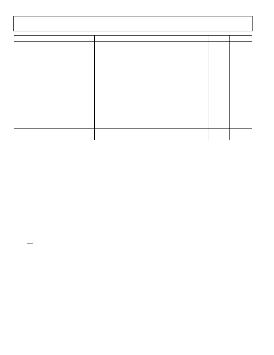
Mnemonic
Description
Bytes
Cycles1
SJMP rel
Short jump (relative address)
2
3
JC rel
Jump on carry = 1
2
3
JNC rel
Jump on carry = 0
2
3
JZ rel
Jump on accumulator = 0
2
3
JNZ rel
Jump on accumulator ! = 0
2
3
DJNZ Rn,rel
Decrement register, JNZ relative
2
3
LJMP
Long jump unconditional
3
4
LCALL3 addr16
Long jump to subroutine
3
4
JB bit,rel
Jump on direct bit = 1
3
4
JNB bit,rel
Jump on direct bit = 0
3
4
JBC bit,rel
Jump on direct bit = 1 and clear
3
4
CJNE A,dir,rel
Compare A, direct JNE relative
3
4
CJNE A,#data,rel
Compare A, immediate JNE relative
3
4
CJNE Rn,#data,rel
Compare register, immediate JNE relative
3
4
CJNE @Ri,#data,rel
Compare indirect, immediate JNE relative
3
4
DJNZ dir,rel
Decrement direct byte, JNZ relative
3
4
Miscellaneous
NOP
No operation
1
One cycle is one clock.
2
MOVX instructions are four cycles when they have 0 wait state. Cycles of MOVX instructions are 4 + n cycles when they have n wait states as programmed via EWAIT.
3
LCALL instructions are three cycles when the LCALL instruction comes from an interrupt.
MEMORY ORGANIZATION
The ADuC845, ADuC847, and ADuC848 contain four memory
blocks:
62 kbytes/32 kbytes/8 kbytes of on-chip Flash/EE program
memory
4 kbytes of on-chip Flash/EE data memory
256 bytes of general-purpose RAM
2 kbytes of internal XRAM
Flash/EE Program Memory
The parts provide up to 62 kbytes of Flash/EE program memory
to run user code. All further references to Flash/EE program
memory assume the 62-kbyte option.
When EA is pulled high externally during a power cycle or a
hardware reset, the parts default to code execution from their
internal 62 kbytes of Flash/EE program memory. The parts do
not support the rollover from internal code space to external
code space. No external code space is available on the parts.
Permanently embedded firmware allows code to be serially
downloaded to the 62 kbytes of internal code space via the
UART serial port while the device is in-circuit. No external
hardware is required.
During run time, 56 kbytes of the 62-kbyte program memory
can be reprogrammed. This means that the code space can be
upgraded in the field by using a user-defined protocol running
on the parts, or it can be used as a data memory. For details, see
the Nonvolatile Flash/EE Memory Overview section.
Flash/EE Data Memory
The user has 4 kbytes of Flash/EE data memory available that
can be accessed indirectly by using a group of registers mapped
into the special function register (SFR) space. For details, see
General-Purpose RAM
The general-purpose RAM is divided into two separate
memories, the upper and the lower 128 bytes of RAM. The
lower 128 bytes of RAM can be accessed through direct or
indirect addressing. The upper 128 bytes of RAM can be
accessed only through indirect addressing because it shares the
same address space as the SFR space, which must be accessed
through direct addressing.
The lower 128 bytes of internal data memory are mapped as
shown in Figure 8. The lowest 32 bytes are grouped into four
banks of eight registers addressed as R0 to R7. The next 16 bytes
(128 bits), locations 20H to 2FH above the register banks, form
a block of directly addressable bit locations at Bit Addresses
00H to 7FH. The stack can be located anywhere in the internal
memory address space, and the stack depth can be expanded up
to 2048 bytes.
Reset initializes the stack pointer to location 07H. Any call or
push pre-increments the SP before loading the stack. Therefore,
loading the stack starts from location 08H, which is also the
first register (R0) of Register Bank 1. Thus, if one is going to use
more than one register bank, the stack pointer should be
initialized to an area of RAM not used for data storage.
相关PDF资料 |
PDF描述 |
|---|---|
| VE-B4T-IW | CONVERTER MOD DC/DC 6.5V 100W |
| AT91SAM9261B-CU-999 | IC MCU ARM9 ULT LOW PWR 217LFBGA |
| VE-B4R-IX | CONVERTER MOD DC/DC 7.5V 75W |
| ATMEGA128-16MUR | MCU AVR 128KB FLASH 16MHZ 64QFN |
| VE-B4R-IW | CONVERTER MOD DC/DC 7.5V 100W |
相关代理商/技术参数 |
参数描述 |
|---|---|
| ADUC847BSZ8-5 | 功能描述:IC MCU FLASH W/24BIT ADC 52MQFP RoHS:是 类别:集成电路 (IC) >> 嵌入式 - 微控制器, 系列:MicroConverter® ADuC8xx 标准包装:38 系列:Encore!® XP® 核心处理器:eZ8 芯体尺寸:8-位 速度:5MHz 连通性:IrDA,UART/USART 外围设备:欠压检测/复位,LED,POR,PWM,WDT 输入/输出数:16 程序存储器容量:4KB(4K x 8) 程序存储器类型:闪存 EEPROM 大小:- RAM 容量:1K x 8 电压 - 电源 (Vcc/Vdd):2.7 V ~ 3.6 V 数据转换器:- 振荡器型:内部 工作温度:-40°C ~ 105°C 封装/外壳:20-SOIC(0.295",7.50mm 宽) 包装:管件 其它名称:269-4116Z8F0413SH005EG-ND |
| ADUC848 | 制造商:AD 制造商全称:Analog Devices 功能描述:MicroConverter Multichannel 24-/16-Bit ADCs with Embedded 62 kB Flash and Single-Cycle MCU |
| ADUC848BCP32-3 | 制造商:Analog Devices 功能描述:10 CHANNEL 16 BIT ADC + FLASH 8 BIT UP - Trays |
| ADUC848BCP32-5 | 制造商:Analog Devices 功能描述:10 CHANNEL 16 BIT ADC + FLASH 8 BIT UP - Trays |
| ADUC848BCP62-3 | 制造商:Analog Devices 功能描述:MCU 8-Bit ADuC8xx 8052 CISC 62KB Flash 3.3V/5V 56-Pin LFCSP EP 制造商:Rochester Electronics LLC 功能描述:8BIT CISC 62KB FLASH 12.85MHZ 3.3V 56LFCSP - Bulk |
发布紧急采购,3分钟左右您将得到回复。