- 您现在的位置:买卖IC网 > PDF目录235794 > AGLE600V2-FFG256C FPGA, 13824 CLBS, 600000 GATES, PBGA256 PDF资料下载
参数资料
| 型号: | AGLE600V2-FFG256C |
| 元件分类: | FPGA |
| 英文描述: | FPGA, 13824 CLBS, 600000 GATES, PBGA256 |
| 封装: | 17 X 17 MM, 1.60 MM HEIGHT, 1 MM PITCH, FBGA-256 |
| 文件页数: | 66/156页 |
| 文件大小: | 5023K |
| 代理商: | AGLE600V2-FFG256C |
第1页第2页第3页第4页第5页第6页第7页第8页第9页第10页第11页第12页第13页第14页第15页第16页第17页第18页第19页第20页第21页第22页第23页第24页第25页第26页第27页第28页第29页第30页第31页第32页第33页第34页第35页第36页第37页第38页第39页第40页第41页第42页第43页第44页第45页第46页第47页第48页第49页第50页第51页第52页第53页第54页第55页第56页第57页第58页第59页第60页第61页第62页第63页第64页第65页当前第66页第67页第68页第69页第70页第71页第72页第73页第74页第75页第76页第77页第78页第79页第80页第81页第82页第83页第84页第85页第86页第87页第88页第89页第90页第91页第92页第93页第94页第95页第96页第97页第98页第99页第100页第101页第102页第103页第104页第105页第106页第107页第108页第109页第110页第111页第112页第113页第114页第115页第116页第117页第118页第119页第120页第121页第122页第123页第124页第125页第126页第127页第128页第129页第130页第131页第132页第133页第134页第135页第136页第137页第138页第139页第140页第141页第142页第143页第144页第145页第146页第147页第148页第149页第150页第151页第152页第153页第154页第155页第156页
IGLOOe DC and Switching Characteristics
Ad vance v0.3
2-3
I/O Power-Up and Supply Voltage Thresholds for Power-On Reset
(Commercial and Industrial)
Sophisticated power-up management circuitry is designed into every IGLOOe device. These circuits
ensure easy transition from the powered-off state to the powered-up state of the device. The many
different supplies can power up in any sequence with minimized current spikes or surges. In
addition, the I/O will be in a known state through the power-up sequence. The basic principle is
shown in Figure 2-1 on page 2-4 and Figure 2-2 on page 2-5.
There are five regions to consider during power-up.
IGLOOe I/Os are activated only if ALL of the following three conditions are met:
2. VCCI > VCC – 0.75 V (typical)
3. Chip is in the operating mode.
VCCI Trip Point:
Ramping up: 0.6 V < trip_point_up < 1.2 V
Ramping down: 0.5 V < trip_point_down < 1.1 V
VCC Trip Point:
Ramping up: 0.6 V < trip_point_up < 1.1 V
Ramping down: 0.5 V < trip_point_down < 1 V
VCC and VCCI ramp-up trip points are about 100 mV higher than ramp-down trip points. This
specifically built-in hysteresis prevents undesirable power-up oscillations and current surges. Note
the following:
During programming, I/Os become tristated and weakly pulled up to VCCI.
JTAG supply, PLL power supplies, and charge pump VPUMP supply have no influence on I/O
behavior.
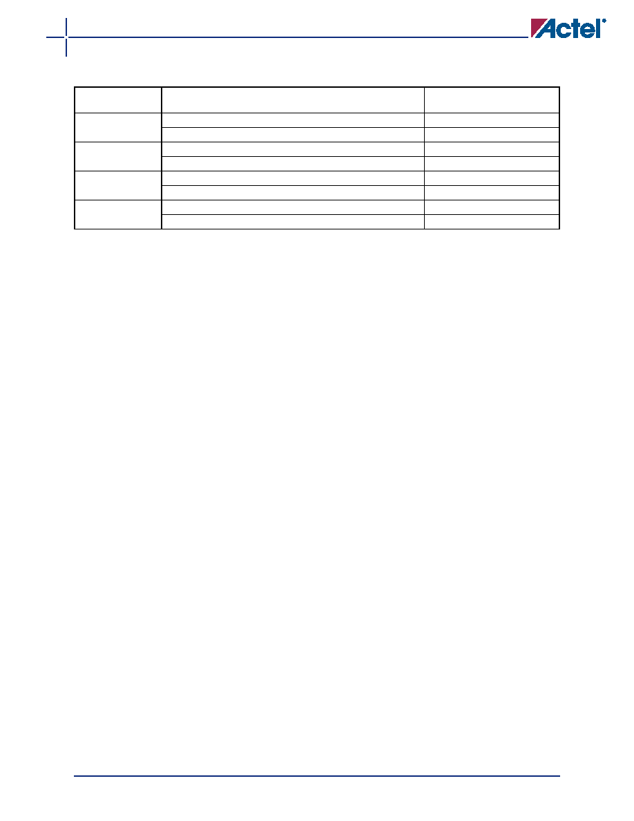
Table 2-4
Overshoot and Undershoot Limits 1
VCCI
Average VCCI–GND Overshoot or Undershoot Duration
as a Percentage of Clock Cycle2
Maximum Overshoot/
Undershoot2
2.7 V or less
10%
1.4 V
5%
1.49 V
3 V
10%
1.1 V
5%
1.19 V
3.3 V
10%
0.79 V
5%
0.88 V
3.6 V
10%
0.45 V
5%
0.54 V
Notes:
1. Based on reliability requirements at junction temperature at 85°C.
2. The duration is allowed at one out of six clock cycles. If the overshoot/undershoot occurs at one out of two
cycles, the maximum overshoot/undershoot has to be reduced by 0.15 V.
3. The device meets overshoot/undershoot specification requirements for PCI inputs with VCCI = 3.45 V at 85°C
maximum, whereas the average toggling of inputs at one-sixth of PCI frequency is considered.
相关PDF资料 |
PDF描述 |
|---|---|
| AGLE600V2-FFG484C | FPGA, 13824 CLBS, 600000 GATES, PBGA484 |
| AGLE600V2-FFGG256C | FPGA, 13824 CLBS, 600000 GATES, PBGA256 |
| AGLE600V2-FFGG484C | FPGA, 13824 CLBS, 600000 GATES, PBGA256 |
| AGLE600V2-FG256C | FPGA, 13824 CLBS, 600000 GATES, PBGA256 |
| AGLE600V2-FGG256C | FPGA, 13824 CLBS, 600000 GATES, PBGA256 |
相关代理商/技术参数 |
参数描述 |
|---|---|
| AGLE600V2-FFG896 | 制造商:ACTEL 制造商全称:Actel Corporation 功能描述:IGLOOe Low-Power Flash FPGAs with Flash Freeze Technology |
| AGLE600V2-FFG896ES | 制造商:ACTEL 制造商全称:Actel Corporation 功能描述:IGLOOe Low-Power Flash FPGAs with Flash Freeze Technology |
| AGLE600V2-FFG896I | 制造商:ACTEL 制造商全称:Actel Corporation 功能描述:IGLOOe Low-Power Flash FPGAs with Flash Freeze Technology |
| AGLE600V2-FFG896PP | 制造商:ACTEL 制造商全称:Actel Corporation 功能描述:IGLOOe Low-Power Flash FPGAs with Flash Freeze Technology |
| AGLE600V2-FFGG896 | 制造商:ACTEL 制造商全称:Actel Corporation 功能描述:IGLOOe Low-Power Flash FPGAs with Flash Freeze Technology |
发布紧急采购,3分钟左右您将得到回复。