- 您现在的位置:买卖IC网 > PDF目录294981 > AGLN030V2-FQNG48 FPGA, PQCC48 PDF资料下载
参数资料
| 型号: | AGLN030V2-FQNG48 |
| 元件分类: | FPGA |
| 英文描述: | FPGA, PQCC48 |
| 封装: | 6 X 6 MM, 0.90 HEIGHT, 0.40 MM PITCH, ROHS COMPLIANT, QFN-48 |
| 文件页数: | 24/114页 |
| 文件大小: | 3991K |
| 代理商: | AGLN030V2-FQNG48 |
第1页第2页第3页第4页第5页第6页第7页第8页第9页第10页第11页第12页第13页第14页第15页第16页第17页第18页第19页第20页第21页第22页第23页当前第24页第25页第26页第27页第28页第29页第30页第31页第32页第33页第34页第35页第36页第37页第38页第39页第40页第41页第42页第43页第44页第45页第46页第47页第48页第49页第50页第51页第52页第53页第54页第55页第56页第57页第58页第59页第60页第61页第62页第63页第64页第65页第66页第67页第68页第69页第70页第71页第72页第73页第74页第75页第76页第77页第78页第79页第80页第81页第82页第83页第84页第85页第86页第87页第88页第89页第90页第91页第92页第93页第94页第95页第96页第97页第98页第99页第100页第101页第102页第103页第104页第105页第106页第107页第108页第109页第110页第111页第112页第113页第114页
IGLOO nano DC and Switching Characteristics
Ad vance v0.2
2-3
I/O Power-Up and Supply Voltage Thresholds for Power-On Reset
(Commercial and Industrial)
Sophisticated power-up management circuitry is designed into every IGLOO nano device. These
circuits ensure easy transition from the powered-off state to the powered-up state of the device.
The many different supplies can power up in any sequence with minimized current spikes or surges.
In addition, the I/O will be in a known state through the power-up sequence. The basic principle is
shown in Figure 2-1 on page 2-4.
There are five regions to consider during power-up.
IGLOO nano I/Os are activated only if ALL of the following three conditions are met:
2. VCCI > VCC – 0.75 V (typical)
3. Chip is in the operating mode.
VCCI Trip Point:
Ramping up (V5 devices): 0.6 V < trip_point_up < 1.2 V
Ramping down (V5 devices): 0.5 V < trip_point_down < 1.1 V
Ramping up (V2 devices): 0.75 V < trip_point_up < 1.05 V
Ramping down (V2 devices): 0.65 V < trip_point_down < 0.95 V
VCC Trip Point:
Ramping up (V5 devices): 0.6 V < trip_point_up < 1.1 V
Ramping down (V5 devices): 0.5 V < trip_point_down < 1.0 V
Ramping up (V2 devices): 0.65 V < trip_point_up < 1.05 V
Ramping down (V2 devices): 0.55 V < trip_point_down < 0.95 V
VCC and VCCI ramp-up trip points are about 100 mV higher than ramp-down trip points. This
specifically built-in hysteresis prevents undesirable power-up oscillations and current surges. Note
the following:
During programming, I/Os become tristated and weakly pulled up to VCCI.
JTAG supply, PLL power supplies, and charge pump VPUMP supply have no influence on I/O
behavior.
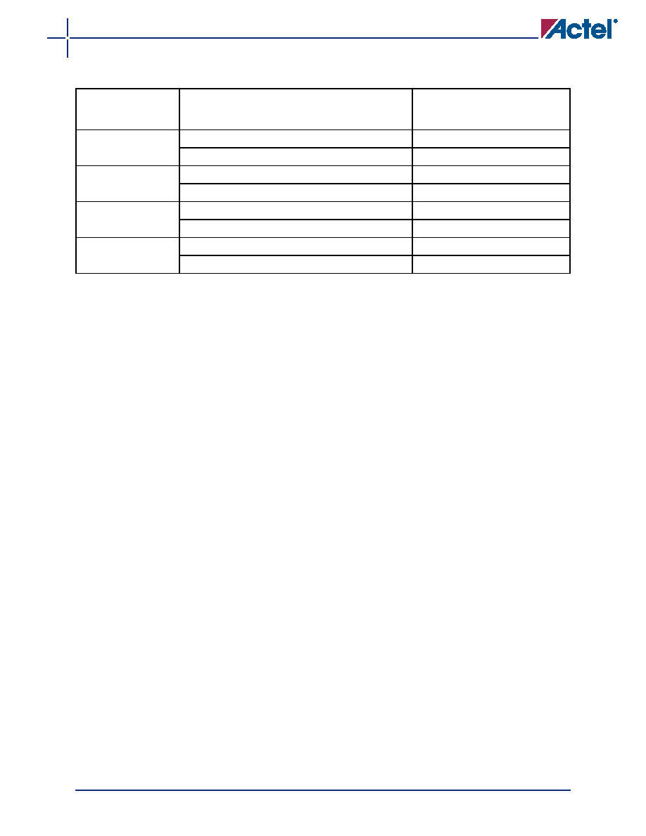
Table 2-4
Overshoot and Undershoot Limits 1
VCCI
Average VCCI–GND Overshoot or
Undershoot Duration
as a Percentage of Clock Cycle2
Maximum Overshoot/
Undershoot2
2.7 V or less
10%
1.4 V
5%
1.49 V
3 V
10%
1.1 V
5%
1.19 V
3.3 V
10%
0.79 V
5%
0.88 V
3.6 V
10%
0.45 V
5%
0.54 V
Notes:
1. Based on reliability requirements at 85°C.
2. The duration is allowed at one out of six clock cycles. If the overshoot/undershoot occurs at one out of two
cycles, the maximum overshoot/undershoot has to be reduced by 0.15 V.
相关PDF资料 |
PDF描述 |
|---|---|
| AGLN030V2-FQNG68 | FPGA, PQCC68 |
| AGLN030V2-FUC81 | FPGA, PBGA81 |
| AGLN030V2-FUCG81 | FPGA, PBGA81 |
| AGLN030V2-FVQ100 | FPGA, PQFP100 |
| AGLN030V2-FVQG100 | FPGA, PQFP100 |
相关代理商/技术参数 |
参数描述 |
|---|---|
| AGLN030V2-ZCSG81 | 功能描述:IC FPGA NANO 1KB 30K 81-CSP RoHS:是 类别:集成电路 (IC) >> 嵌入式 - FPGA(现场可编程门阵列) 系列:IGLOO nano 标准包装:152 系列:IGLOO PLUS LAB/CLB数:- 逻辑元件/单元数:792 RAM 位总计:- 输入/输出数:120 门数:30000 电源电压:1.14 V ~ 1.575 V 安装类型:表面贴装 工作温度:-40°C ~ 85°C 封装/外壳:289-TFBGA,CSBGA 供应商设备封装:289-CSP(14x14) |
| AGLN030V2-ZCSG81I | 功能描述:IC FPGA NANO 1KB 30K 81-CSP RoHS:是 类别:集成电路 (IC) >> 嵌入式 - FPGA(现场可编程门阵列) 系列:IGLOO nano 标准包装:152 系列:IGLOO PLUS LAB/CLB数:- 逻辑元件/单元数:792 RAM 位总计:- 输入/输出数:120 门数:30000 电源电压:1.14 V ~ 1.575 V 安装类型:表面贴装 工作温度:-40°C ~ 85°C 封装/外壳:289-TFBGA,CSBGA 供应商设备封装:289-CSP(14x14) |
| AGLN030V2-ZQNG48 | 功能描述:IC FPGA NANO 1KB 30K 48-QFN RoHS:是 类别:集成电路 (IC) >> 嵌入式 - FPGA(现场可编程门阵列) 系列:IGLOO nano 标准包装:152 系列:IGLOO PLUS LAB/CLB数:- 逻辑元件/单元数:792 RAM 位总计:- 输入/输出数:120 门数:30000 电源电压:1.14 V ~ 1.575 V 安装类型:表面贴装 工作温度:-40°C ~ 85°C 封装/外壳:289-TFBGA,CSBGA 供应商设备封装:289-CSP(14x14) |
| AGLN030V2-ZQNG48I | 功能描述:IC FPGA NANO 1KB 30K 48-QFN RoHS:是 类别:集成电路 (IC) >> 嵌入式 - FPGA(现场可编程门阵列) 系列:IGLOO nano 标准包装:152 系列:IGLOO PLUS LAB/CLB数:- 逻辑元件/单元数:792 RAM 位总计:- 输入/输出数:120 门数:30000 电源电压:1.14 V ~ 1.575 V 安装类型:表面贴装 工作温度:-40°C ~ 85°C 封装/外壳:289-TFBGA,CSBGA 供应商设备封装:289-CSP(14x14) |
| AGLN030V2-ZQNG68 | 功能描述:IC FPGA NANO 1KB 30K 68-QFN RoHS:是 类别:集成电路 (IC) >> 嵌入式 - FPGA(现场可编程门阵列) 系列:IGLOO nano 标准包装:152 系列:IGLOO PLUS LAB/CLB数:- 逻辑元件/单元数:792 RAM 位总计:- 输入/输出数:120 门数:30000 电源电压:1.14 V ~ 1.575 V 安装类型:表面贴装 工作温度:-40°C ~ 85°C 封装/外壳:289-TFBGA,CSBGA 供应商设备封装:289-CSP(14x14) |
发布紧急采购,3分钟左右您将得到回复。