参数资料
| 型号: | AGLP125V2-CSG289I |
| 厂商: | Microsemi SoC |
| 文件页数: | 43/134页 |
| 文件大小: | 0K |
| 描述: | IC FPGA IGLOO PLUS 125K 289-CSP |
| 标准包装: | 152 |
| 系列: | IGLOO PLUS |
| 逻辑元件/单元数: | 3120 |
| RAM 位总计: | 36864 |
| 输入/输出数: | 212 |
| 门数: | 125000 |
| 电源电压: | 1.14 V ~ 1.575 V |
| 安装类型: | 表面贴装 |
| 工作温度: | -40°C ~ 85°C |
| 封装/外壳: | 289-TFBGA,CSBGA |
| 供应商设备封装: | 289-CSP(14x14) |
第1页第2页第3页第4页第5页第6页第7页第8页第9页第10页第11页第12页第13页第14页第15页第16页第17页第18页第19页第20页第21页第22页第23页第24页第25页第26页第27页第28页第29页第30页第31页第32页第33页第34页第35页第36页第37页第38页第39页第40页第41页第42页当前第43页第44页第45页第46页第47页第48页第49页第50页第51页第52页第53页第54页第55页第56页第57页第58页第59页第60页第61页第62页第63页第64页第65页第66页第67页第68页第69页第70页第71页第72页第73页第74页第75页第76页第77页第78页第79页第80页第81页第82页第83页第84页第85页第86页第87页第88页第89页第90页第91页第92页第93页第94页第95页第96页第97页第98页第99页第100页第101页第102页第103页第104页第105页第106页第107页第108页第109页第110页第111页第112页第113页第114页第115页第116页第117页第118页第119页第120页第121页第122页第123页第124页第125页第126页第127页第128页第129页第130页第131页第132页第133页第134页
IGLOO PLUS DC and Switching Characteristics
2-2
Revision 16
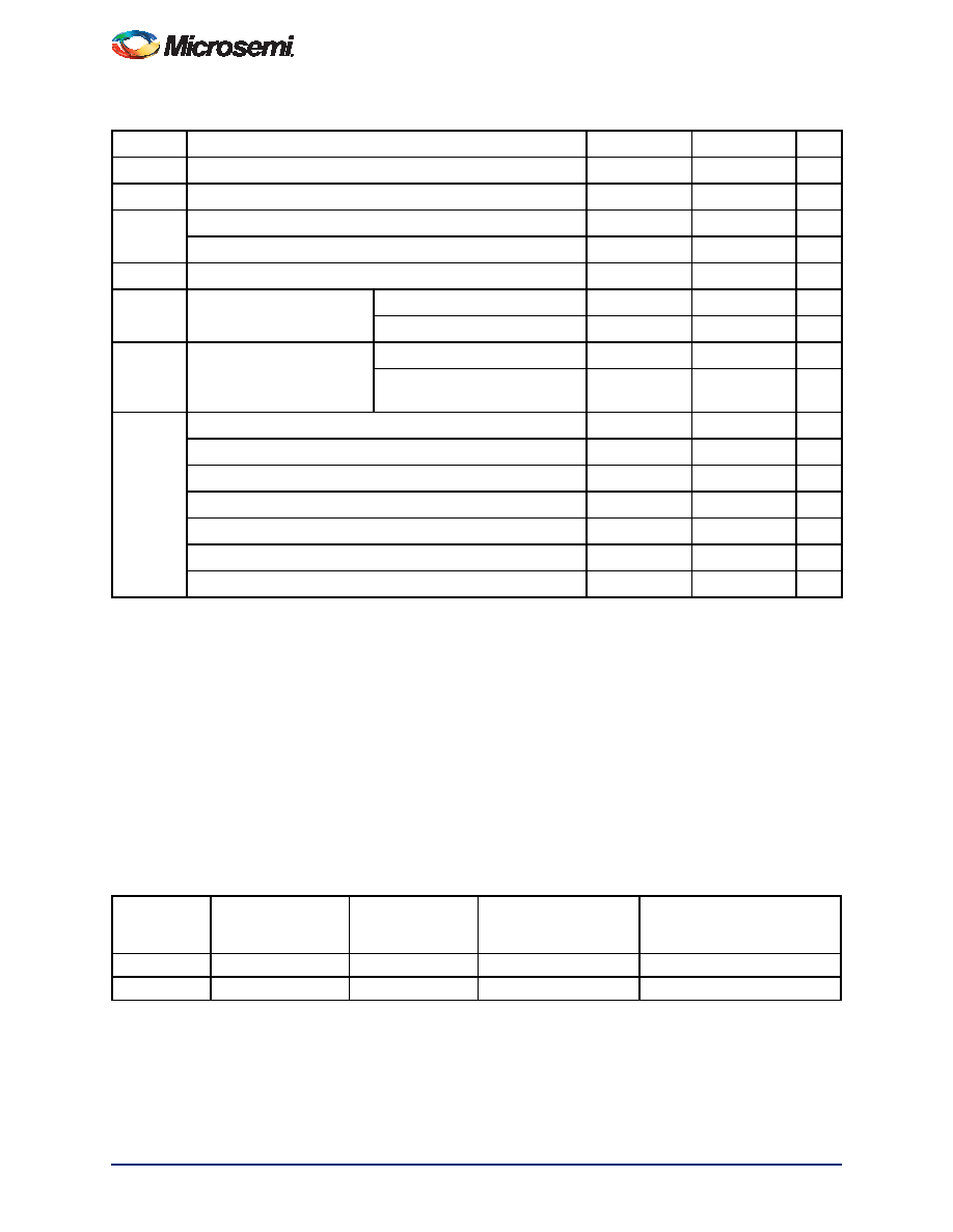
Table 2-2 Recommended Operating Conditions1,2
Symbol
Parameter
Commercial
Industrial
Units
TA
Ambient temperature
0 to +70
–40 to +85
°C
TJ
Junction temperature2
0 to + 85
–40 to +100
°C
VCC3
1.5 V DC core supply voltage 4
1.425 to 1.575
V
1.2 V–1.5 V wide range core voltage5,6
1.14 to 1.575
V
VJTAG
JTAG DC voltage
1.4 to 3.6
V
VPUMP7
Programming voltage
Programming mode
3.15 to 3.45
V
Operation
0 to 3.6
V
VCCPLL8 Analog power supply (PLL)
1.5 V DC core supply voltage4
1.425 to 1.575
V
1.2 V–1.5 V wide range core
voltage5
1.14 to 1.575
V
VCCI
1.2 V DC supply voltage5
1.14 to 1.26
V
1.2 V DC wide range supply voltage5
1.14 to 1.575
V
1.5 V DC supply voltage
1.425 to 1.575
V
1.8 V DC supply voltage
1.7 to 1.9
V
2.5 V DC supply voltage
2.3 to 2.7
V
3.3 V wide range DC supply voltage9
2.7 to 3.6
V
3.3 V DC supply voltage
3.0 to 3.6
V
Notes:
1. All parameters representing voltages are measured with respect to GND unless otherwise specified.
2. To ensure targeted reliability standards are met across ambient and junction operating temperatures, Microsemi
recommends that the user follow best design practices using Microsemi’s timing and power simulation tools.
3. The ranges given here are for power supplies only. The recommended input voltage ranges specific to each I/O
standard are given in Table 2-21 on page 2-19. VCCI should be at the same voltage within a given I/O bank.
4. For IGLOO PLUS V5 devices
5. For IGLOO PLUS V2 devices only, operating at VCCI
VCC.
6. All IGLOO PLUS devices (V5 and V2) must be programmed with the VCC core voltage at 1.5 V. Applications using V2
devices powered by a 1.2 V supply must switch the core supply to 1.5 V for in-system programming.
7. VPUMP can be left floating during operation (not programming mode).
8. VCCPLL pins should be tied to VCC pins. See the Pin Descriptions chapter of the IGLOO PLUS FPGA Fabric User’s
Guide for further information.
9. 3.3 V wide range is compliant to the JDEC8b specification and supports 3.0 V VCCI operation.
Table 2-3 Flash Programming Limits – Retention, Storage, and Operating Temperature 1
Product
Grade
Programming
Cycles
Program
Retention
(biased/unbiased)
Maximum Storage
Temperature TSTG
(°C) 2
Maximum Operating
Junction
Temperature TJ (°C) 2
Commercial
500
20 years
110
100
Industrial
500
20 years
110
100
Notes:
1. This is a stress rating only; functional operation at any condition other than those indicated is not implied.
2. These limits apply for program/data retention only. Refer to Table 2-1 on page 2-1 and Table 2-2 for device operating
conditions and absolute limits.
相关PDF资料 |
PDF描述 |
|---|---|
| ASC43DREH-S734 | CONN EDGECARD 86POS .100 EYELET |
| M1A3P1000-FG256 | IC FPGA M1 1KB FLASH 1M 256FBGA |
| FMC13DREN | CONN EDGECARD 26POS .100 EYELET |
| APA150-BG456 | IC FPGA PROASIC+ 150K 456-PBGA |
| FMC13DREH | CONN EDGECARD 26POS .100 EYELET |
相关代理商/技术参数 |
参数描述 |
|---|---|
| AGLP125-V2CSG289PP | 制造商:ACTEL 制造商全称:Actel Corporation 功能描述:IGLOO PLUS Low-Power Flash FPGAs with FlashFreeze Technology |
| AGLP125-V2FCS289 | 制造商:ACTEL 制造商全称:Actel Corporation 功能描述:IGLOO PLUS Low-Power Flash FPGAs with FlashFreeze Technology |
| AGLP125-V2FCS289ES | 制造商:ACTEL 制造商全称:Actel Corporation 功能描述:IGLOO PLUS Low-Power Flash FPGAs with FlashFreeze Technology |
| AGLP125-V2FCS289I | 制造商:ACTEL 制造商全称:Actel Corporation 功能描述:IGLOO PLUS Low-Power Flash FPGAs with FlashFreeze Technology |
| AGLP125-V2FCS289PP | 制造商:ACTEL 制造商全称:Actel Corporation 功能描述:IGLOO PLUS Low-Power Flash FPGAs with FlashFreeze Technology |
发布紧急采购,3分钟左右您将得到回复。