- 您现在的位置:买卖IC网 > PDF目录166212 > AM29F017D (Spansion Inc.) 16 Megabit (2 M x 8-Bit) CMOS 5.0 Volt-only, Uniform Sector Flash Memory PDF资料下载
参数资料
| 型号: | AM29F017D |
| 厂商: | Spansion Inc. |
| 英文描述: | 16 Megabit (2 M x 8-Bit) CMOS 5.0 Volt-only, Uniform Sector Flash Memory |
| 中文描述: | 16兆位(2米× 8位)的CMOS 5.0伏只,统一部门快闪记忆体 |
| 文件页数: | 19/44页 |
| 文件大小: | 1021K |
| 代理商: | AM29F017D |
第1页第2页第3页第4页第5页第6页第7页第8页第9页第10页第11页第12页第13页第14页第15页第16页第17页第18页当前第19页第20页第21页第22页第23页第24页第25页第26页第27页第28页第29页第30页第31页第32页第33页第34页第35页第36页第37页第38页第39页第40页第41页第42页第43页第44页
Am29F017D
25
ABSOLUTE MAXIMUM RATINGS
Storage Temperature
Plastic Packages . . . . . . . . . . . . . . . –65
°C to +125°C
Ambient Temperature
with Power Applied. . . . . . . . . . . . . . –55
°C to +125°C
Voltage with Respect to Ground
VCC (Note 1) . . . . . . . . . . . . . . . . . –2.0 V to 7.0 V
A9, OE#, RESET# (Note 2) . . . . . –2.0 V to 12.5 V
All other pins (Note 1) . . . . . . . . . . –2.0 V to 7.0 V
Output Short Circuit Current (Note 3) . . . . . . 200 mA
Notes:
1. Minimum DC voltage on input or I/O pins is –0.5 V. During
voltage transitions, inputs may overshoot VSS to –2.0 V
for periods of up to 20 ns. See Figure 6. Maximum DC
voltage on output and I/O pins is VCC + 0.5 V. During
voltage transitions, outputs may overshoot to VCC + 2.0 V
for periods up to 20 ns. See Figure 7.
2. Minimum DC input voltage on A9, OE#, RESET# pins is
–0.5V. During voltage transitions, A9, OE#, RESET# pins
may overshoot VSS to –2.0 V for periods of up to 20 ns.
See Figure 6. Maximum DC input voltage on A9, OE#,
and RESET# is 12.5 V which may overshoot to 13.5 V for
periods up to 20 ns.
3. No more than one output shorted at a time. Duration of
the short circuit should not be greater than one second.
Stresses greater than those listed in this section may cause
permanent damage to the device. This is a stress rating
only; functional operation of the device at these or any other
conditions above those indicated in the operational sections
of this specification is not implied. Exposure of the device to
absolute maximum rating conditions for extended periods
may affect device reliability.
OPERATING RANGES
Commercial (C) Devices
Ambient Temperature (TC) . . . . . . . . . . . 0°C to +70°C
Industrial (I) Devices
Ambient Temperature (TC) . . . . . . . . . –40°C to +85°C
Extended (E) Devices
Ambient Temperature (TA) . . . . . . . . –55°C to +125°C
VCC Supply Voltages
VCC for ± 10% all devices . . . . . . . . .+4.5 V to +5.5 V
Operating ranges define those limits between which the
functionality of the device is guaranteed.
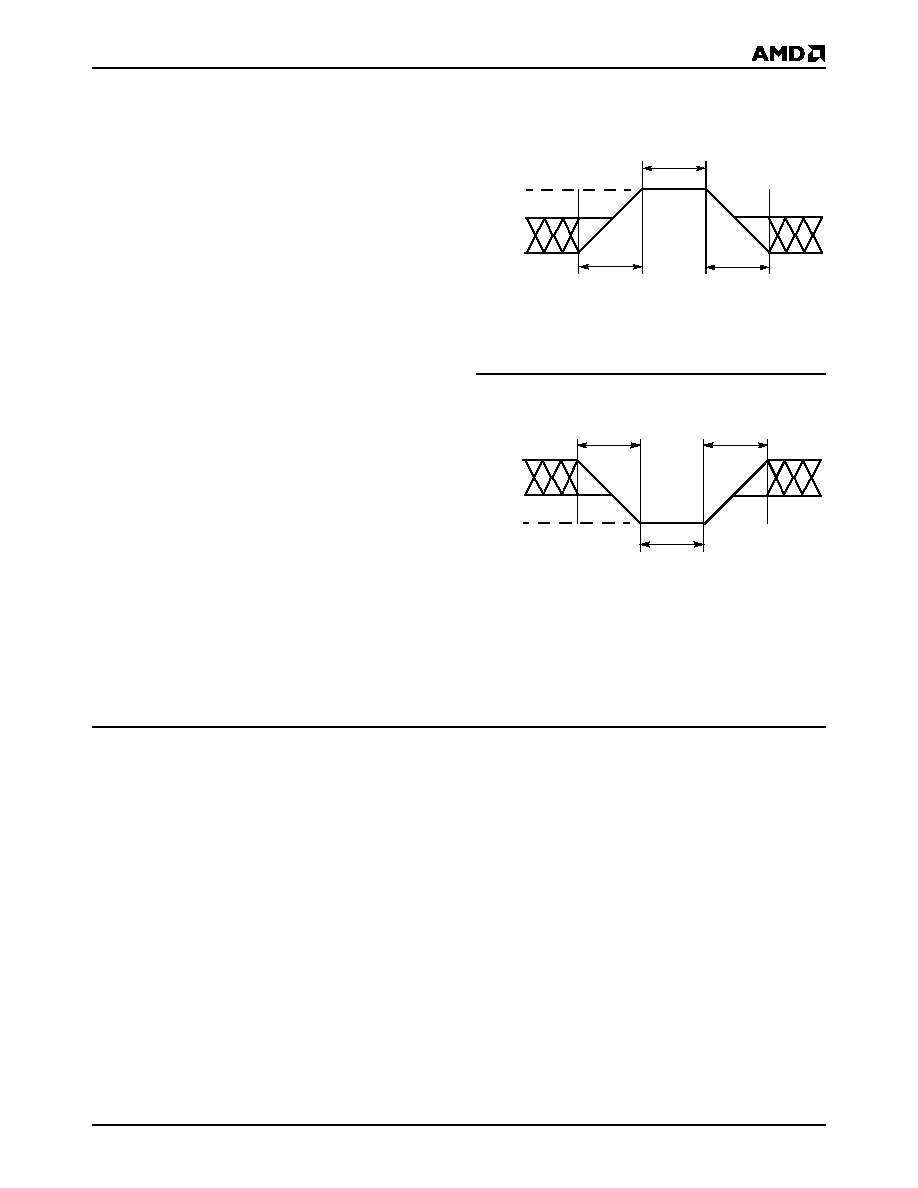
20 ns
VCC
+2.0 V
VCC
+0.5 V
20 ns
2.0 V
Figure 6.
Maximum Negative
Overshoot Waveform
20 ns
+0.8 V
–0.5 V
20 ns
–2.0 V
Figure 7.
Maximum Positive
Overshoot Waveform
相关PDF资料 |
PDF描述 |
|---|---|
| AM29F017D-120 | 16 Megabit (2 M x 8-Bit) CMOS 5.0 Volt-only, Uniform Sector Flash Memory |
| AM29F032B-150SE | 4M X 8 FLASH 5V PROM, 150 ns, PDSO44 |
| AM29F032B-75FC | 4M X 8 FLASH 5V PROM, 70 ns, PDSO40 |
| AM29F080-120SEB | 1M X 8 FLASH 5V PROM, 120 ns, PDSO44 |
| AM29F080-150EEB | 1M X 8 FLASH 5V PROM, 150 ns, PDSO40 |
相关代理商/技术参数 |
参数描述 |
|---|---|
| AM29F017D-120EC | 制造商:Spansion 功能描述:FLASH PARALLEL 5V 16MBIT 2MX8 120NS 48TSOP - Trays |
| AM29F017D-70FI | 制造商:Spansion 功能描述:FLASH PARALLEL 5V 16MBIT 2MX8 70NS 48TSOP - Trays |
| am29f017d-90fc/t | 制造商:Advanced Micro Devices 功能描述: |
| AM29F032B-120ED | 制造商:Spansion 功能描述: |
| AM29F032B75ED | 制造商:Advanced Micro Devices 功能描述: |
发布紧急采购,3分钟左右您将得到回复。