- 您现在的位置:买卖IC网 > PDF目录166215 > AM29F800BT-70ED (SPANSION LLC) Flash Memory IC; Memory Size:8Mbit; Memory Configuration:512K x 16 / 1M x 8; Package/Case:48-TSOP; Leaded Process Compatible:Yes; Peak Reflow Compatible (260 C):Yes; Supply Voltage Max:5V; Access Time, Tacc:70ns RoHS Compliant: Yes PDF资料下载
参数资料
| 型号: | AM29F800BT-70ED |
| 厂商: | SPANSION LLC |
| 元件分类: | PROM |
| 英文描述: | Flash Memory IC; Memory Size:8Mbit; Memory Configuration:512K x 16 / 1M x 8; Package/Case:48-TSOP; Leaded Process Compatible:Yes; Peak Reflow Compatible (260 C):Yes; Supply Voltage Max:5V; Access Time, Tacc:70ns RoHS Compliant: Yes |
| 中文描述: | 512K X 16 FLASH 5V PROM, 70 ns, PDSO48 |
| 封装: | LEAD FREE, MO-142DD, TSOP-48 |
| 文件页数: | 3/45页 |
| 文件大小: | 1402K |
| 代理商: | AM29F800BT-70ED |
第1页第2页当前第3页第4页第5页第6页第7页第8页第9页第10页第11页第12页第13页第14页第15页第16页第17页第18页第19页第20页第21页第22页第23页第24页第25页第26页第27页第28页第29页第30页第31页第32页第33页第34页第35页第36页第37页第38页第39页第40页第41页第42页第43页第44页第45页
March 3, 2009 21504E6
Am29F800B
9
D A TA SH EE T
DEVICE BUS OPERATIONS
This section describes the requirements and use of the
device bus operations, which are initiated through the
internal command register. The command register it-
self does not occupy any addressable memory loca-
tion. The register is composed of latches that store the
commands, along with the address and data informa-
tion needed to execute the command. The contents of
the register serve as inputs to the internal state ma-
chine. The state machine outputs dictate the function of
the device. The appropriate device bus operations
table lists the inputs and control levels required, and the
resulting output. The following subsections describe
each of these operations in further detail.
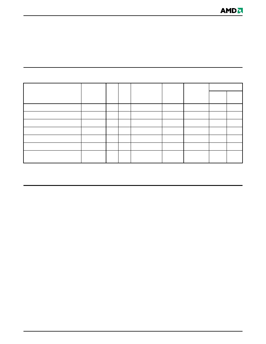
Table 1.
Am29F800B Device Bus Operations
Legend:
L = Logic Low = VIL, H = Logic High = VIH, VID = 12.0 ± 0.5 V, X = Don’t Care, DIN = Data In, DOUT = Data Out, AIN = Address In
Note: See the sections on Sector Group Protection and Temporary Sector Unprotect for more information.
Word/Byte Configuration
The BYTE# pin controls whether the device data I/O
pins DQ15–DQ0 operate in the byte or word configura-
tion. If the BYTE# pin is set at logic ‘1’, the device is in
word configuration, DQ15–DQ0 are active and con-
trolled by CE# and OE#.
If the BYTE# pin is set at logic ‘0’, the device is in byte
configuration, and only data I/O pins DQ0–DQ7 are ac-
tive and controlled by CE# and OE#. The data I/O pins
DQ8–DQ14 are tri-stated, and the DQ15 pin is used as
an input for the LSB (A-1) address function.
Requirements for Reading Array Data
To read array data from the outputs, the system must
drive the CE# and OE# pins to VIL. CE# is the power
control and selects the device. OE# is the output control
and gates array data to the output pins. WE# should re-
main at VIH.
The internal state machine is set for reading array
data upon device power-up, or after a hardware reset.
This ensures that no spurious alteration of the mem-
ory content occurs during the power transition. No
command is necessary in this mode to obtain array
data. Standard microprocessor read cycles that as-
sert valid addresses on the device address inputs
produce valid data on the device data outputs. The
device remains enabled for read access until the
command register contents are altered.
See “Reading Array Data” for more information. Refer
to the AC Read Operations table for timing specifica-
tions and to the Read Operations Timings diagram for
the timing waveforms. ICC1 in the DC Characteristics
table represents the active current specification for
reading array data.
Writing Commands/Command Sequences
To write a command or command sequence (which in-
cludes programming data to the device and erasing
sectors of memory), the system must drive WE# and
CE# to VIL, and OE# to VIH.
An erase operation can erase one sector, multiple sec-
tors, or the entire device. The Sector Address Tables in-
dicate the address space that each sector occupies. A
“sector address” consists of the address bits required
to uniquely select a sector. See the “Command Defini-
Operation
CE#
OE#
WE#
RESET#
A0–A18
DQ0–DQ7
DQ8–DQ15
BYTE#
= VIH
BYTE#
= VIL
Read
L
H
AIN
DOUT
High-Z
Write
L
H
L
H
AIN
DIN
High-Z
CMOS Standby
VCC ± 0.5 V
X
VCC ± 0.5 V
X
High-Z
TTL Standby
H
X
H
X
High-Z
Output Disable
L
H
X
High-Z
Hardware Reset
X
L
X
High-Z
Temporary Sector Unprotect
(See Note)
X
VID
AIN
DIN
X
相关PDF资料 |
PDF描述 |
|---|---|
| AM29F800BT-90ED | Flash Memory IC; Memory Size:8Mbit; Memory Configuration:512K x 16 / 1M x 8; Package/Case:48-TSOP; Leaded Process Compatible:Yes; Peak Reflow Compatible (260 C):Yes; Supply Voltage Max:5V; Access Time, Tacc:90ns RoHS Compliant: Yes |
| AM29F800BT-90EF | Flash Memory IC; Leaded Process Compatible:Yes; Memory Size:8Mbit; Package/Case:48-TSOP; Peak Reflow Compatible (260 C):Yes; Supply Voltage Max:5V; Access Time, Tacc:90ns; Series:AM29 RoHS Compliant: Yes |
| AM29F800BT-90SD | Flash Memory IC; Leaded Process Compatible:Yes; Memory Size:8Mbit; Package/Case:44-SOIC; Peak Reflow Compatible (260 C):Yes; Supply Voltage Max:5V; Access Time, Tacc:90ns; Series:AM29 RoHS Compliant: Yes |
| AM29F800BB-120EC | Dual Retriggerable Monostable Multivibrators 16-VQFN -40 to 85 |
| AM29F800BB-55EF | Flash Memory IC; Leaded Process Compatible:Yes; Memory Size:8Mbit; Package/Case:48-TSOP; Peak Reflow Compatible (260 C):Yes; Supply Voltage Max:5V; Access Time, Tacc:55ns; Series:AM29 RoHS Compliant: Yes |
相关代理商/技术参数 |
参数描述 |
|---|---|
| AM29F800BT-70ED | 制造商:Spansion 功能描述:FLASH MEMORY IC |
| AM29F800BT70EF | 制造商: 功能描述: 制造商:undefined 功能描述: |
| AM29F800BT-70EF | 功能描述:闪存 8M (1MX8/512KX16) Parallel NOR Fl 5V RoHS:否 制造商:ON Semiconductor 数据总线宽度:1 bit 存储类型:Flash 存储容量:2 MB 结构:256 K x 8 定时类型: 接口类型:SPI 访问时间: 电源电压-最大:3.6 V 电源电压-最小:2.3 V 最大工作电流:15 mA 工作温度:- 40 C to + 85 C 安装风格:SMD/SMT 封装 / 箱体: 封装:Reel |
| AM29F800BT-70EF/T | 制造商:Spansion 功能描述:8M (1MX8/512KX16) 5V, BOOT BLOCK, TOP, TSOP48, IND, HAZMAT - Tape and Reel |
| AM29F800BT-70EF\\T | 制造商:Spansion 功能描述:IC 8MEG(512K16)BOTTOM SECTOR 100K(CS39S) |
发布紧急采购,3分钟左右您将得到回复。