- 您现在的位置:买卖IC网 > PDF目录166215 > AM29LV004BB-90ED (SPANSION LLC) Flash Memory IC; Leaded Process Compatible:Yes; Memory Size:4Mbit; Package/Case:48-TSOP; Peak Reflow Compatible (260 C):Yes; Supply Voltage Max:3V; Access Time, Tacc:90ns; Series:AM29 RoHS Compliant: Yes PDF资料下载
参数资料
| 型号: | AM29LV004BB-90ED |
| 厂商: | SPANSION LLC |
| 元件分类: | PROM |
| 英文描述: | Flash Memory IC; Leaded Process Compatible:Yes; Memory Size:4Mbit; Package/Case:48-TSOP; Peak Reflow Compatible (260 C):Yes; Supply Voltage Max:3V; Access Time, Tacc:90ns; Series:AM29 RoHS Compliant: Yes |
| 中文描述: | 512K X 8 FLASH 3V PROM, 90 ns, PDSO40 |
| 封装: | LEAD FREE, MO-142CD, TSOP-40 |
| 文件页数: | 8/39页 |
| 文件大小: | 681K |
| 代理商: | AM29LV004BB-90ED |
第1页第2页第3页第4页第5页第6页第7页当前第8页第9页第10页第11页第12页第13页第14页第15页第16页第17页第18页第19页第20页第21页第22页第23页第24页第25页第26页第27页第28页第29页第30页第31页第32页第33页第34页第35页第36页第37页第38页第39页
16
Am29LV004B
21522D5 October 11, 2006
D A TA SH EE T
Characteristics” for parameters, and to Figure 15 for
timing diagrams.
Note: See Table 5 for program command sequence.
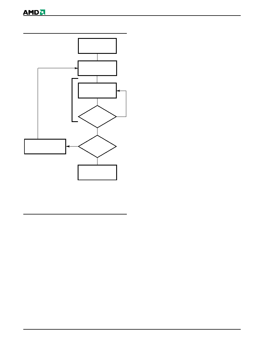
Figure 3.
Program Operation
Chip Erase Command Sequence
Chip erase is a six bus cycle operation. The chip erase
command sequence is initiated by writing two unlock
cycles, followed by a set-up command. Two additional
unlock write cycles are then followed by the chip erase
command, which in turn invokes the Embedded Erase
algorithm. The device does not require the system to
preprogram prior to erase. The Embedded Erase algo-
rithm automatically preprograms and verifies the entire
memory for an all zero data pattern prior to electrical
erase. The system is not required to provide any con-
trols or timings during these operations. Table 5 shows
the address and data requirements for the chip erase
command sequence.
Any co mm an ds w r itt en to th e ch ip d ur ing the
Embedded Erase algorithm are ignored. Note that a
hardware reset during the chip erase operation imme-
diately terminates the operation. The Chip Erase
command sequence should be reinitiated once the
device has returned to reading array data, to ensure
data integrity.
The system can determine the status of the erase oper-
ation by using DQ7, DQ6, DQ2, or RY/BY#. See “Write
Operation Status” for information on these status bits.
When the Embedded Erase algorithm is complete, the
device returns to reading array data and addresses are
no longer latched.
Figure 4 illustrates the algorithm for the erase opera-
tion. See the Erase/Program Operations tables in “AC
Characteristics” for parameters, and to Figure 16 for
timing diagrams.
Sector Erase Command Sequence
Sector erase is a six bus cycle operation. The sector
erase command sequence is initiated by writing two
unlock cycles, followed by a set-up command. Two
additional unlock write cycles are then followed by the
address of the sector to be erased, and the sector
erase command. Table 5 shows the address and data
requirements for the sector erase command sequence.
The device does not require the system to preprogram
the memory prior to erase. The Embedded Erase algo-
rithm automatically programs and verifies the sector for
an all zero data pattern prior to electrical erase. The
system is not required to provide any controls or
timings during these operations.
After the command sequence is written, a sector erase
time-out of 50 s begins. During the time-out period,
additional sector addresses and sector erase com-
mands may be written. Loading the sector erase buffer
may be done in any sequence, and the number of
sectors may be from one sector to all sectors. The time
between these additional cycles must be less than 50
μs, otherwise the last address and command might not
be accepted, and erasure may begin. It is recom-
mended that processor interrupts be disabled during
this time to ensure all commands are accepted. The
interrupts can be re-enabled after the last Sector Erase
command is written. If the time between additional
sector erase commands can be assumed to be less
than 50 s, the system need not monitor DQ3. Any
command other than Sector Erase or Erase
Suspend during the time-out period resets the
device to reading array data. The system must
rewrite the command sequence and any additional
sector addresses and commands.
The system can monitor DQ3 to determine if the sector
erase timer has timed out. (See the “DQ3: Sector Erase
Timer” section.) The time-out begins from the rising
edge of the final WE# pulse in the command sequence.
Once the sector erase operation has begun, only the
Erase Suspend command is valid. All other commands
are ignored. Note that a hardware reset during the
START
Write Program
Command Sequence
Data Poll
from System
Verify Data?
No
Yes
Last Address?
No
Yes
Programming
Completed
Increment Address
Embedded
Program
algorithm
in progress
相关PDF资料 |
PDF描述 |
|---|---|
| AM29LV004BB-90EF | Flash Memory IC; Leaded Process Compatible:Yes; Memory Size:4Mbit; Package/Case:48-TSOP; Peak Reflow Compatible (260 C):Yes; Supply Voltage Max:3V; Access Time, Tacc:90ns; Series:AM29 RoHS Compliant: Yes |
| AM29LV004BT-120ED | Flash Memory IC; Leaded Process Compatible:Yes; Memory Size:4Mbit; Package/Case:48-TSOP; Peak Reflow Compatible (260 C):Yes; Supply Voltage Max:3V; Access Time, Tacc:120ns; Series:AM29 RoHS Compliant: Yes |
| AM29LV004BT-120EF | Flash Memory IC; Leaded Process Compatible:Yes; Memory Size:4Mbit; Package/Case:48-TSOP; Peak Reflow Compatible (260 C):Yes; Supply Voltage Max:3V; Access Time, Tacc:120ns; Series:AM29 RoHS Compliant: Yes |
| AM29LV004BT-70ED | Flash Memory IC; Leaded Process Compatible:Yes; Memory Size:4Mbit; Package/Case:48-TSOP; Peak Reflow Compatible (260 C):Yes; Supply Voltage Max:3V; Access Time, Tacc:70ns; Series:AM29 RoHS Compliant: Yes |
| AM29LV004BT-70EF | Flash Memory IC; Leaded Process Compatible:Yes; Memory Size:4Mbit; Package/Case:48-TSOP; Peak Reflow Compatible (260 C):Yes; Supply Voltage Max:3V; Access Time, Tacc:70ns; Series:AM29 RoHS Compliant: Yes |
相关代理商/技术参数 |
参数描述 |
|---|---|
| am29lv004bt-120ed | 制造商:Advanced Micro Devices 功能描述: |
| AM29LV004BT-90EI | 制造商:Advanced Micro Devices 功能描述: |
| AM29LV008BB-120ECT | 制造商:Spansion 功能描述:IC 8MEG X8, 3 V FLASH BOTTOM B |
| AM29LV008BB-120ED | 制造商:Spansion 功能描述:IC SM FLASH 3V 8MB |
| AM29LV008BB-120ED | 制造商:Spansion 功能描述:FLASH MEMORY IC |
发布紧急采购,3分钟左右您将得到回复。