参数资料
| 型号: | APA150-BG456 |
| 厂商: | Microsemi SoC |
| 文件页数: | 68/178页 |
| 文件大小: | 0K |
| 描述: | IC FPGA PROASIC+ 150K 456-PBGA |
| 标准包装: | 24 |
| 系列: | ProASICPLUS |
| RAM 位总计: | 36864 |
| 输入/输出数: | 242 |
| 门数: | 150000 |
| 电源电压: | 2.3 V ~ 2.7 V |
| 安装类型: | 表面贴装 |
| 工作温度: | 0°C ~ 70°C |
| 封装/外壳: | 456-BBGA |
| 供应商设备封装: | 456-PBGA(35x35) |
第1页第2页第3页第4页第5页第6页第7页第8页第9页第10页第11页第12页第13页第14页第15页第16页第17页第18页第19页第20页第21页第22页第23页第24页第25页第26页第27页第28页第29页第30页第31页第32页第33页第34页第35页第36页第37页第38页第39页第40页第41页第42页第43页第44页第45页第46页第47页第48页第49页第50页第51页第52页第53页第54页第55页第56页第57页第58页第59页第60页第61页第62页第63页第64页第65页第66页第67页当前第68页第69页第70页第71页第72页第73页第74页第75页第76页第77页第78页第79页第80页第81页第82页第83页第84页第85页第86页第87页第88页第89页第90页第91页第92页第93页第94页第95页第96页第97页第98页第99页第100页第101页第102页第103页第104页第105页第106页第107页第108页第109页第110页第111页第112页第113页第114页第115页第116页第117页第118页第119页第120页第121页第122页第123页第124页第125页第126页第127页第128页第129页第130页第131页第132页第133页第134页第135页第136页第137页第138页第139页第140页第141页第142页第143页第144页第145页第146页第147页第148页第149页第150页第151页第152页第153页第154页第155页第156页第157页第158页第159页第160页第161页第162页第163页第164页第165页第166页第167页第168页第169页第170页第171页第172页第173页第174页第175页第176页第177页第178页
ProASICPLUS Flash Family FPGAs
2- 6
v5.9
Input/Output Blocks
To meet complex system demands, the ProASICPLUS
family offers devices with a large number of user I/O
pins; up to 712 on the APA1000. Table 2-3 shows the
available supply voltage configurations (the PLL block
uses an independent 2.5 V supply on the AVDD and
AGND pins). All I/Os include ESD protection circuits. Each
I/O has been tested to 2000 V to the human body model
(per JESD22 (HBM)).
Six or seven standard I/O pads are grouped with a GND
pad and either a VDD (core power) or VDDP (I/O power)
pad. Two reference bias signals circle the chip. One
protects the cascaded output drivers, while the other
creates a virtual VDD supply for the I/O ring.
I/O pads are fully configurable to provide the maximum
flexibility and speed. Each pad can be configured as an
input, an output, a tristate driver, or a bidirectional
buffer (Figure 2-6 and Table 2-4).
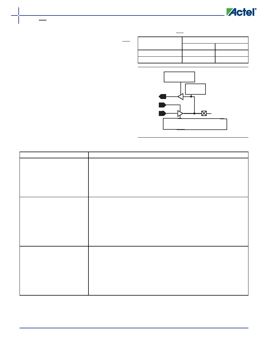
Table 2-3
ProASICPLUS I/O Power Supply Voltages
VDDP
2.5 V
3.3 V
Input Compatibility
2.5V
3.3V
Output Drive
2.5V
3.3V
Figure 2-6 I/O Block Schematic Representation
3.3 V / 2.5 V
Signal Control
Pull-up
Control
Pad
Y
EN
A
3.3 V / 2.5 V Signal Control Drive
Strength and Slew-Rate Control
Table 2-4
I/O Features
Function
Description
I/O pads configured as inputs
Selectable 2.5 V or 3.3 V threshold levels
Optional pull-up resistor
Optionally configurable as Schmitt trigger input. The Schmitt trigger input option can be
configured as an input only, not a bidirectional buffer. This input type may be slower than
a standard input under certain conditions and has a typical hysteresis of 0.35 V. I/O macros
with an "S" in the standard I/O library have added Schmitt capabilities.
3.3 V PCI Compliant (except Schmitt trigger inputs)
I/O pads configured as outputs
Selectable 2.5 V or 3.3 V compliant output signals
2.5 V – JEDEC JESD 8-5
3.3 V – JEDEC JESD 8-A (LVTTL and LVCMOS)
3.3 V PCI compliant
Ability to drive LVTTL and LVCMOS levels
Selectable drive strengths
Selectable slew rates
Tristate
I/O pads configured as bidirectional
buffers
Selectable 2.5 V or 3.3 V compliant output signals
2.5 V – JEDEC JESD 8-5
3.3 V – JEDEC JESD 8-A (LVTTL and LVCMOS)
3.3 V PCI compliant
Optional pull-up resistor
Selectable drive strengths
Selectable slew rates
Tristate
相关PDF资料 |
PDF描述 |
|---|---|
| FMC13DREH | CONN EDGECARD 26POS .100 EYELET |
| APA150-BGG456 | IC FPGA PROASIC+ 150K 456-PBGA |
| ABM43DTMS | CONN EDGECARD 86POS R/A .156 SLD |
| APA150-PQG208A | IC FPGA PROASIC+ 150K 208-PQFP |
| ABM43DTBS | CONN EDGECARD 86POS R/A .156 SLD |
相关代理商/技术参数 |
参数描述 |
|---|---|
| APA150-BG456I | 功能描述:IC FPGA PROASIC+ 150K 456-PBGA RoHS:否 类别:集成电路 (IC) >> 嵌入式 - FPGA(现场可编程门阵列) 系列:ProASICPLUS 标准包装:40 系列:SX-A LAB/CLB数:6036 逻辑元件/单元数:- RAM 位总计:- 输入/输出数:360 门数:108000 电源电压:2.25 V ~ 5.25 V 安装类型:表面贴装 工作温度:0°C ~ 70°C 封装/外壳:484-BGA 供应商设备封装:484-FPBGA(27X27) |
| APA150-BGB | 制造商:ACTEL 制造商全称:Actel Corporation 功能描述:ProASIC Flash Family FPGAs |
| APA150-BGES | 制造商:ACTEL 制造商全称:Actel Corporation 功能描述:ProASIC Flash Family FPGAs |
| APA150-BGG456 | 功能描述:IC FPGA PROASIC+ 150K 456-PBGA RoHS:是 类别:集成电路 (IC) >> 嵌入式 - FPGA(现场可编程门阵列) 系列:ProASICPLUS 标准包装:90 系列:ProASIC3 LAB/CLB数:- 逻辑元件/单元数:- RAM 位总计:36864 输入/输出数:157 门数:250000 电源电压:1.425 V ~ 1.575 V 安装类型:表面贴装 工作温度:-40°C ~ 125°C 封装/外壳:256-LBGA 供应商设备封装:256-FPBGA(17x17) |
| APA150-BGG456I | 功能描述:IC FPGA PROASIC+ 150K 456-PBGA RoHS:是 类别:集成电路 (IC) >> 嵌入式 - FPGA(现场可编程门阵列) 系列:ProASICPLUS 标准包装:40 系列:SX-A LAB/CLB数:6036 逻辑元件/单元数:- RAM 位总计:- 输入/输出数:360 门数:108000 电源电压:2.25 V ~ 5.25 V 安装类型:表面贴装 工作温度:0°C ~ 70°C 封装/外壳:484-BGA 供应商设备封装:484-FPBGA(27X27) |
发布紧急采购,3分钟左右您将得到回复。