参数资料
| 型号: | AS1369-BWLT-33 |
| 厂商: | ams |
| 文件页数: | 4/22页 |
| 文件大小: | 0K |
| 描述: | IC REG LDO 3.3V .2A 4WLCSP |
| 标准包装: | 1 |
| 稳压器拓扑结构: | 正,固定式 |
| 输出电压: | 3.3V |
| 输入电压: | 最高 5.5V |
| 电压 - 压降(标准): | 0.08V @ 200mA |
| 稳压器数量: | 1 |
| 电流 - 输出: | 200mA |
| 电流 - 限制(最小): | 210mA |
| 工作温度: | -40°C ~ 85°C |
| 安装类型: | 表面贴装 |
| 封装/外壳: | 4-UFBGA,WLCSP |
| 供应商设备封装: | 4-WLCSP |
| 包装: | 标准包装 |
| 其它名称: | AS1369-BWLT-33DKR |
�� �
�
�AS1369�
�Datasheet� -� A� b� s� o� l� u� t� e� M� a� x� i� m� u� m� R� a� t� i� n� g� s�
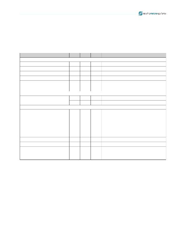
�5� Absolute� Maximum� Ratings�
�Stresses� beyond� those� listed� in� Table� 2� may� cause� permanent� damage� to� the� device.� These� are� stress� ratings� only,� and� functional� operation� of�
�the� device� at� these� or� any� other� conditions� beyond� those� indicated� in� Electrical� Characteristics� on� page� 4� is� not� implied.� Exposure� to� absolute�
�maximum� rating� conditions� for� extended� periods� may� affect� device� reliability.�
�Table� 2.� Absolute� Maximum� Ratings�
�1�
�Parameter�
�Min�
�Max�
�Units�
�Comments�
�Electrical� Parameters�
�Input/Output� Voltage�
�Input� Supply� Voltage�
�Shutdown� Input� Voltage�
�Output� Voltage�
�I� OUT�
�2�
�-0.3�
�-0.3�
�-0.3�
�-0.3�
�+7�
�+7�
�+7�
�+7�
�V�
�V�
�V�
�V�
�Short-circuit� protected�
�Latch-Up�
�-100�
�+100�
�mA�
�Norm:� JEDEC� 78�
�Electrostatic� Discharge�
�ESD�
�2�
�500�
�kV�
�V�
�Norm:� MIL� 883� E� method� 3015�
�CDM� JESD22-C101C� methods�
�Temperature� Ranges� and� Storage� Conditions�
�Thermal� Resistance,� ?� JA�
�3�
�345�
�oC/W�
�The� maximum� allowable� power� dissipation� is� a� function� of� the�
�maximum� junction� temperature� (T� J(MAX� ),� the� junction-to-�
�ambient� thermal� resistance� (� ?� JA� ),� and� the� ambient�
�temperature� (T� AMB� ).� The� maximum� allowable� power�
�dissipation� at� any� ambient� temperature� is� calculated� as:�
�P� (MAX)� =� (T� J(MAX)� -� (T� AMB� ))/� ?� JA� (EQ� 1)�
�Where:�
�The� value� of� ?� JA� for� the� WLP� package� is� 345°C/W.�
�Operating� Junction� Temperature�
�Storage� Temperature� Range�
�-40�
�-65�
�+125�
�+150�
�oC�
�oC�
�Package� Body� Temperature�
�+260�
�oC�
�The� reflow� peak� soldering� temperature� (body� temperature)�
�specified� is� in� accordance� with� IPC/JEDEC� J-STD-020�
�“Moisture/Reflow� Sensitivity� Classification� for� Non-Hermetic�
�Solid� State� Surface� Mount� Devices”.�
�1.� The� AS1369� uses� an� internal� protective� structure� against� light� influence.� However,� exposing� the� WLP� package� to� direct� light� could�
�cause� device� malfunction.�
�2.� The� output� PNP� structure� contains� a� diode� between� pins� V� IN� and� V� OUT� that� is� normally� reverse-biased.� reversing� the� polarity� of� pins�
�V� IN� and� V� OUT� will� activate� this� diode.�
�3.� Exceeding� the� maximum� allowable� dissipation� will� cause� excessive� device� temperature� and� the� regulator� will� go� into� thermal� shutdown.�
�www.austriamicrosystems.com/LDOs/AS1369�
�Revision� 1.7�
�3� -� 21�
�相关PDF资料 |
PDF描述 |
|---|---|
| RCM22DTMN-S189 | CONN EDGECARD 44POS R/A .156 SLD |
| 400USC470MEFCSN30X45 | CAP ALUM 470UF 400V 20% SNAP-IN |
| 63MXG8200MEFCSN30X40 | CAP ALUM 8200UF 63V 20% SNAP-IN |
| 80MXC5600MEFCSN30X45 | CAP ALUM 5600UF 80V 20% SNAP-IN |
| EBM36DTMN-S189 | CONN EDGECARD 72POS R/A .156 SLD |
相关代理商/技术参数 |
参数描述 |
|---|---|
| AS1369-BWLT-33-10K | 制造商:AMS 功能描述:IC REG LDO 3.3V 0.2A 4WLCSP |
| AS1369BWLT33-10K | 制造商:AMS 功能描述:IC REG LDO 3.3V 0.2A 4WLCSP |
| AS1369BWLT33-1K | 制造商:AMS 功能描述:IC REG LDO 3.3V 0.2A 4WLCSP |
| AS1369-BWLT-45 | 制造商:AMSCO 制造商全称:austriamicrosystems AG 功能描述:200mA Ultra-Compact Low Dropout Regulator |
| AS1369-BWLT-50 | 制造商:AMSCO 制造商全称:austriamicrosystems AG 功能描述:200mA Ultra-Compact Low Dropout Regulator |
发布紧急采购,3分钟左右您将得到回复。