参数资料
| 型号: | AS3543-ECTP |
| 厂商: | ams |
| 文件页数: | 80/92页 |
| 文件大小: | 0K |
| 描述: | IC CODEC AUDIO FRONT END 68CTBGA |
| 标准包装: | 4,000 |
| 类型: | 音频编解码器 |
| 应用: | 便携式音频,电话 |
| 安装类型: | 表面贴装 |
| 封装/外壳: | 68-TFBGA |
| 供应商设备封装: | 68-CTBGA(6x6) |
| 包装: | 带卷 (TR) |
第1页第2页第3页第4页第5页第6页第7页第8页第9页第10页第11页第12页第13页第14页第15页第16页第17页第18页第19页第20页第21页第22页第23页第24页第25页第26页第27页第28页第29页第30页第31页第32页第33页第34页第35页第36页第37页第38页第39页第40页第41页第42页第43页第44页第45页第46页第47页第48页第49页第50页第51页第52页第53页第54页第55页第56页第57页第58页第59页第60页第61页第62页第63页第64页第65页第66页第67页第68页第69页第70页第71页第72页第73页第74页第75页第76页第77页第78页第79页当前第80页第81页第82页第83页第84页第85页第86页第87页第88页第89页第90页第91页第92页
www.austriamicrosystems.com
Revision 1.11
80 - 91
AS3543 3v2
Data Sheet - R e g i s t e r D e f i n i t i o n
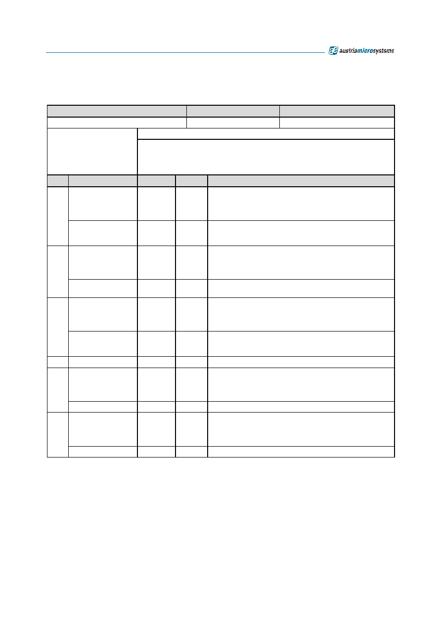
Table 83. Second Interrupt Register
Name
Base
Default
IRQENRD_1
2-wire serial
00h
Offset: 24h
Second Interrupt Register
Please be aware that writing to this register will enable/disable the
corresponding interrupts, while reading gets the actual interrupt status and
will clear the register at the same time. It is not possible to read back the
interrupt enable/disable settings. This register is reset at a AVDD27-POR.
Bit
Bit Name
Default
Access
Bit Description
7
PWRUP_IRQ
0
W
Enables interrupt which is invoked whenever a high signal at
the PWRUP input pin occurs
0: disable
1: enable
x
R
This bit is set whenever a high level of min. BVDD/3 at the
PWRUP input pin occurs (PWRUP pin is commonly connected
to the power-up button)
6
WAKEUP_IRQ
0
W
Enables interrupt which is invoked whenever a wake-up from
RTC wake-up counter occurs
0: disable
1: enable
x
R
This bit is set when a wake-up has been invoked by the RTC
wake-up counter.
5
MCLK_IRQ
0
W
Enables interrupt which is invoked whenever a high signal at
the MCLK input pin occurs
0: disable
1: enable
x
R
This bit is set whenever a high level of min. BVDD/3 at the
MCLK input pin occurs (MCLK pin can be used as alternative
power-up button)
4:2
-
0
n/a
1
CVDD2_SD
0
W
Invokes shut-down of AFE when a –10% under-voltage spike
at CVDD2 occurs
0: disable
1: enable
CVDD2_under
x
R
This bit is set when a –5% under-voltage at CVDD2 occurs
0
CVDD2_IRQ
0
W
Enables interrupt for over-voltage/under-voltage supervision of
CVDD2
0: disable
1: enable
CVDD2_over
x
R
This bit is set when a +8% over-voltage at CVDD2 occurs
ams
AG
Technical
content
still
valid
相关PDF资料 |
PDF描述 |
|---|---|
| ASM2I9940LG-32LT | IC CLK BUFFER 2:18 250MHZ 32LQFP |
| ASM3P2780AF-06OR | IC FREQ MOD 4X EMI REDUCT 6TSOP |
| AT42QT1011-MAH | IC SENSR TOUCH/PROX 1CH 8-UDFN |
| AT42QT2161-MMU | IC TOUCH SENSOR 16KEY 28QFN |
| B300W35A102E1G | IC PROCESSOR AUDIO 24BIT WLCSP |
相关代理商/技术参数 |
参数描述 |
|---|---|
| AS35490FLF | 制造商:TT Electronics / IRC 功能描述:AS35490FLF |
| AS35490HLF | 制造商:TT Electronics / IRC 功能描述:AS35490HLF |
| AS35490JLF | 制造商:TT Electronics / IRC 功能描述:AS35490JLF |
| AS35491FLF | 制造商:TT Electronics / IRC 功能描述:AS35491FLF |
| AS35491HLF | 制造商:TT Electronics / IRC 功能描述:AS35491HLF |
发布紧急采购,3分钟左右您将得到回复。