- 您现在的位置:买卖IC网 > PDF目录166232 > AS5SS256K18DQ-10/XT (AUSTIN SEMICONDUCTOR INC) 256K x 18 SSRAM Synchronous Burst SRAM, Flow-Through PDF资料下载
参数资料
| 型号: | AS5SS256K18DQ-10/XT |
| 厂商: | AUSTIN SEMICONDUCTOR INC |
| 元件分类: | SRAM |
| 英文描述: | 256K x 18 SSRAM Synchronous Burst SRAM, Flow-Through |
| 中文描述: | 256K X 18 STANDARD SRAM, 10 ns, PQFP100 |
| 封装: | TQFP-100 |
| 文件页数: | 6/13页 |
| 文件大小: | 135K |
| 代理商: | AS5SS256K18DQ-10/XT |
AS5SS256K18
Rev. 2.1 06/05
Austin Semiconductor, Inc. reserves the right to change products or specifications without notice.
2
SSRAM
AS5SS256K18
Austin Semiconductor, Inc.
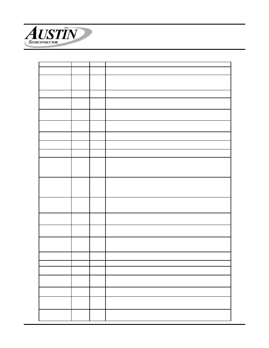
PIN DESCRIPTIONS
PIN NUMBERS
SYM
TYPE
DESCRIPTION
37, 36, 32-35, 44-50,
80-82, 99, 100
SA0, SA1,
SA
Input
Synchronous Address Inputs: These inputs are registered and must meet the setup and
hold times around the rising edge of CLK.
93, 94
BWa\
BWb\
Input
Synchronous Byte Write Enables: These active LOW inputs allow individual bytes to be
written and must meet the setup and hold times around the rising edge of CLK. A byte
write enables is LOW for a WRITE cycle and HIGH for a READ cycle. BWa\ controls DQa
pins and DQPa; BWb\ controls DQb pins and DQPb.
87
BWE\
Input
Byte Write Enable: This active LOW input permits BYTE WRITE operations and must meet
the setup and hold times around the rising edge of CLK.
88
GW\
Input
Global Write: This active LOW input allows a full 18-bit WRITE to occur independent of the
BWE\ and BWx\ lines and must meet the setup and hold times around the rising edge of
CLK.
89
CLK
Input
Clock: This signal registers the addresses, data, chip enables, byte write enables and burst
control inputs on its rising edge. All synchronous inputs must meet setup and hold times
around the clock’s rising edge.
98
CE\
Input
Synchronous Chip Enable: This active LOW input is used to enable the device and
Conditions the internal use of ADSP\. CE\ is sampled only when a new external address is
loaded.
92
CE2\
Input
Synchronous Chip Enable: This active LOW input is used to enable the device and is
sampled only when a new external address is loaded.
97
CE2
Input
Synchronous Chip Enable: This active HIGH input is used to enable the device and is
sampled only when a new external address is loaded.
86
OE\
Input
Output Enable: This active LOW, asynchronous input enables the data I/O output drivers.
83
ADV\
Input
Synchronous Address Advance: This active LOW input is used to advance the internal
burst counter, controlling burst access after the external address is loaded. A HIGH on this
pin effectively causes wait states to be generated (no address advance). To ensure use of
correct address during WRITE cycle, ADV\ must be HIGH at the rising edge of the first
clock after an ADSP\ cycle is initiated.
84
ADSP\
Input
Synchronous Address Status Processor: This active LOW input interrupts any ongoing
burst, causing a new external address to be registered. A READ is performed using the
new address, independent of the byte write enables and ADSC\, but dependent upon CE\,
CE2, and CE2\. ADSP\ is ignored if CE\ is HIGH. Power-down state is entered if CE2 if
LOW or CE2\ is HIGH.
85
ADSC\
Input
Synchronous Address Status Controller: This active LOW input interrupts any ongoing
burst, causing a new external address to be registered. A READ or WRITE is performed
using the new address if CE\ is LOW. ADSC\ is also used to place the chip into power-
down state when CE\ is HIGH.
31
MODE
Input
Mode: This input selects the burst sequence. A LOW on this pin selects LINEAR BURST. A
NC or HIGH on this pin selects INTERLEAVED BURST. Do not alter input state while
device is operating.
64
ZZ
Input
Snooze Enable: This active HIGH, asynchronous input causes the device to enter a low-
power standby mode in which all data in the memory array is retained. When ZZ is active,
all other inputs are ignored.
(a) 58, 59, 62, 63, 68,
69, 72, 73
(b) 8, 9, 12,13, 18, 19,
22, 23
DQa
DQb
Input/
Output
SRAM Data I/Os: Byte "a" is DQa pins; Byte "b" is DQb pins. Input data must meet setup
and hold times around the rising edge of CLK.
74, 24
NC/DQPa
NC/DQPb
NC/ I/O
No Connect/Parity Data I/Os: Byte "a" is DQPa pins; Byte "b" is DQPb pins.
15, 41,65, 91
VDD
Supply
Power Supply: See DC Electrical Characteristics and Operating Conditions for range.
4, 11, 20, 27, 54, 61,
70, 77
VDDQ
Supply
Isolated Output Buffer Supply: See DC Electrical Characterics and Operating Conditions for
range.
5, 10, 14, 17, 21, 26,
40, 55, 60, 67 71, 76,
90
VSS
Supply
Ground: GND
38, 39
DNU
---
Do Not Use: These signals may either be unconnected or wired to GND to improve
package heat dissipation.
1-3, 6, 7, 16,25, 28-30,
51-53, 56,57, 66, 75,
78, 79, 95, 96
NC
-----
No Connect: These signals are not internally connected and may be connected to ground to
improve package heat dissipation.
42, 43
NF
No Function: These pins are internally connected to the die and will have the capacitance of
input pins. It is allowable to leave these pins unconnected or driven by signals.
相关PDF资料 |
PDF描述 |
|---|---|
| AS5SS256K18DQ-9/IT | 256K x 18 SSRAM Synchronous Burst SRAM, Flow-Through |
| AS5SS256K18DQ-9/XT | 256K x 18 SSRAM Synchronous Burst SRAM, Flow-Through |
| AS5SS256K18DQ-8IT | 256K x 18 SSRAM Synchronous Burst SRAM, Flow-Through |
| AS5SS256K36ADQ-8.5/883C | 256K x 36 SSRAM Flow-Through, Synchronous Burst SRAM |
| AS6054 | 1000 MHz - 6000 MHz RF/MICROWAVE WIDE BAND LOW POWER AMPLIFIER |
相关代理商/技术参数 |
参数描述 |
|---|---|
| AS5SS256K18DQ-8 | 制造商:未知厂家 制造商全称:未知厂家 功能描述:x18 Fast Synchronous SRAM |
| AS5SS256K18DQ-8/IT | 制造商:AUSTIN 制造商全称:Austin Semiconductor 功能描述:256K x 18 SSRAM Synchronous Burst SRAM, Flow-Through |
| AS5SS256K18DQ-8IT | 制造商:AUSTIN 制造商全称:Austin Semiconductor 功能描述:256K x 18 SSRAM Synchronous Burst SRAM, Flow-Through |
| AS5SS256K18DQ-9 | 制造商:未知厂家 制造商全称:未知厂家 功能描述:x18 Fast Synchronous SRAM |
| AS5SS256K18DQ-9/IT | 制造商:AUSTIN 制造商全称:Austin Semiconductor 功能描述:256K x 18 SSRAM Synchronous Burst SRAM, Flow-Through |
发布紧急采购,3分钟左右您将得到回复。