- 您现在的位置:买卖IC网 > PDF目录166232 > AS5SS256K18DQ-9/XT (AUSTIN SEMICONDUCTOR INC) 256K x 18 SSRAM Synchronous Burst SRAM, Flow-Through PDF资料下载
参数资料
| 型号: | AS5SS256K18DQ-9/XT |
| 厂商: | AUSTIN SEMICONDUCTOR INC |
| 元件分类: | SRAM |
| 英文描述: | 256K x 18 SSRAM Synchronous Burst SRAM, Flow-Through |
| 中文描述: | 256K X 18 STANDARD SRAM, 8.5 ns, PQFP100 |
| 封装: | TQFP-100 |
| 文件页数: | 11/13页 |
| 文件大小: | 135K |
| 代理商: | AS5SS256K18DQ-9/XT |
AS5SS256K18
Rev. 2.1 06/05
Austin Semiconductor, Inc. reserves the right to change products or specifications without notice.
7
SSRAM
AS5SS256K18
Austin Semiconductor, Inc.
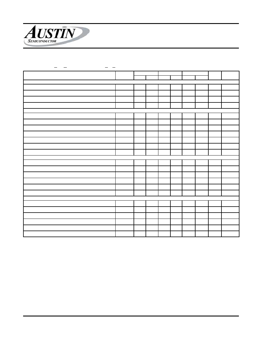
ELECTRICAL CHARACTERISTICS AND RECOMMENDED AC OPERATING CONDITIONS
(Note 1) -55oC < T
A < +125
oC and -40oC<T
A<+85
oC; V
DD = +3.3V +0.3V/-0.165V unless otherwise noted)
MIN
MAX
MIN
MAX
MIN
MAX
Clock cycle time
tKC
8.8
10
15
ns
Clock frequency
tKF
113
100
66
MHz
Clock HIGH time
tKH
2.5
3.0
4.0
ns
2
Clock LOW time
tKL
2.5
3.0
4.0
ns
2
Clock to output valid
tKQ
7.5
8.5
10
ns
Clock to output invalid
tKQX
1.5
3.0
ns
3
Clock to output in Low-Z
tKQLZ
1.5
3.0
ns
3, 4, 5
Clock to output in High-Z
tKQHZ
4.2
5.0
ns
3, 4, 5
OE\ to output valid
tOEQ
4.2
5.0
ns
6
OE\ to output in Low-Z
tOELZ
00
0
ns
3, 4, 5
OE\ to output in High-Z
tOEHZ
4.2
5.0
ns
3, 4, 5
Address
tAS
1.5
1.8
2.0
ns
7, 8
Address status (ADSC\, ADSP\)
tADSS
1.5
1.8
2.0
ns
7, 8
Address advance (ADV\)
tAAS
1.5
1.8
2.0
ns
7, 8
Byte write enables (BWa\-BWb\, GW\, BWE\)
tWS
1.5
1.8
2.0
ns
7, 8
Data-in
tDS
1.5
1.8
2.0
ns
7, 8
Chip enable (CE\)
tCES
1.5
1.8
2.0
ns
7, 8
Address
tAH
0.5
ns
7, 8
Address status (ADSC\, ADSP\)
tADSH
0.5
ns
7, 8
Address advance (ADV\)
tAAH
0.5
ns
7, 8
Byte write enables (BWa\-BWb\, GW\, BWE\)
tWH
0.5
ns
7, 8
Data-in
tDH
0.5
ns
7, 8
Chip enable (CE\)
tCEH
0.5
ns
7, 8
OUTPUT TIMES
SETUP TIMES
HOLD TIMES
NOTES
UNITS
SYMBOL
CLOCK
DESCRIPTION
-9
-8
-10
NOTES:
1. Test conditions as specified with the output loading shown in Figure 1 for 3.3V I/O (VDDQ = +3.3V +0.3V/-0.165V) unless otherwise
noted.
2. Measured as HIGH above V
IH and LOW below VIL.
3. This parameter is measured with the output loading shown in Figure 2 for 3.3V I/O.
4. This parameter is sampled.
5. Transition is measured ±500mV from steady state voltage.
6. OE\ is a “Don’t Care” when a byte write enable is sampled LOW.
7. A READ cycle is defined by byte write enables all HIGH or ADSP\ LOW for the required setup and hold times. A WRITE cycle is
defined by at least one byte write enable LOW and ADSP\ HIGH for the required setup and hold times.
8. This is a synchronous device. All addresses must meet the specified setup and hold times for all rising edges of CLK when either ADSP\ or
ADSC\ is LOW and chip enabled. All other synchronous inputs must meet the setup and hold times with stable logic levels for all rising edges
of clock (CLK) when the chip is enabled. Chip enable must be valid at each rising edge of CLK when either ADSP\ or ADSC\ is LOW to
remain enabled.
相关PDF资料 |
PDF描述 |
|---|---|
| AS5SS256K18DQ-8IT | 256K x 18 SSRAM Synchronous Burst SRAM, Flow-Through |
| AS5SS256K36ADQ-8.5/883C | 256K x 36 SSRAM Flow-Through, Synchronous Burst SRAM |
| AS6054 | 1000 MHz - 6000 MHz RF/MICROWAVE WIDE BAND LOW POWER AMPLIFIER |
| AS7C1028-15JC | 256K X 4 STANDARD SRAM, 15 ns, PDSO28 |
| AS7C25512FT32A-85BIN | 512K X 32 STANDARD SRAM, 8.5 ns, PBGA165 |
相关代理商/技术参数 |
参数描述 |
|---|---|
| AS5SS256K36 | 制造商:AUSTIN 制造商全称:Austin Semiconductor 功能描述:256K x 36 SSRAM Flow-Through, Synchronous Burst SRAM |
| AS5SS256K36_05 | 制造商:AUSTIN 制造商全称:Austin Semiconductor 功能描述:256K x 36 SSRAM Flow-Through, Synchronous Burst SRAM |
| AS5SS256K36A | 制造商:AUSTIN 制造商全称:Austin Semiconductor 功能描述:256K x 36 SSRAM Flow-Through, Synchronous Burst SRAM |
| AS5SS256K36ADQ-10/883C | 制造商:AUSTIN 制造商全称:Austin Semiconductor 功能描述:256K x 36 SSRAM Flow-Through, Synchronous Burst SRAM |
| AS5SS256K36ADQ-10/IT | 制造商:AUSTIN 制造商全称:Austin Semiconductor 功能描述:256K x 36 SSRAM Flow-Through, Synchronous Burst SRAM |
发布紧急采购,3分钟左右您将得到回复。