参数资料
| 型号: | AT32UC3A0256-ALUT |
| 厂商: | Atmel |
| 文件页数: | 91/97页 |
| 文件大小: | 0K |
| 描述: | IC MCU AVR32 256KB FLASH 144LQFP |
| 产品培训模块: | AVR UC3 Audio Application MCU Product Line Introduction AVR EVK1105 Digital Audio Gateway Kit AVR® UC3 Introduction |
| 标准包装: | 300 |
| 系列: | AVR®32 UC3 A0 |
| 核心处理器: | AVR |
| 芯体尺寸: | 32-位 |
| 速度: | 66MHz |
| 连通性: | EBI/EMI,以太网,I²C,SPI,SSC,UART/USART,USB OTG |
| 外围设备: | 欠压检测/复位,POR,PWM,WDT |
| 输入/输出数: | 109 |
| 程序存储器容量: | 256KB(256K x 8) |
| 程序存储器类型: | 闪存 |
| RAM 容量: | 64K x 8 |
| 电压 - 电源 (Vcc/Vdd): | 1.65 V ~ 1.95 V |
| 数据转换器: | A/D 8x10b |
| 振荡器型: | 内部 |
| 工作温度: | -40°C ~ 85°C |
| 封装/外壳: | 144-LQFP |
| 包装: | 托盘 |
| 配用: | ATSTK600-RC33-ND - STK600 ROUTING CARD AVR ATEVK1105-ND - KIT EVAL FOR AT32UC3A0 ATAVRONEKIT-ND - KIT AVR/AVR32 DEBUGGER/PROGRMMR ATEVK1100-ND - KIT DEV/EVAL FOR AVR32 AT32UC3A |
第1页第2页第3页第4页第5页第6页第7页第8页第9页第10页第11页第12页第13页第14页第15页第16页第17页第18页第19页第20页第21页第22页第23页第24页第25页第26页第27页第28页第29页第30页第31页第32页第33页第34页第35页第36页第37页第38页第39页第40页第41页第42页第43页第44页第45页第46页第47页第48页第49页第50页第51页第52页第53页第54页第55页第56页第57页第58页第59页第60页第61页第62页第63页第64页第65页第66页第67页第68页第69页第70页第71页第72页第73页第74页第75页第76页第77页第78页第79页第80页第81页第82页第83页第84页第85页第86页第87页第88页第89页第90页当前第91页第92页第93页第94页第95页第96页第97页
dsPIC30F6010
DS70119E-page 90
2006 Microchip Technology Inc.
15.6
Complementary PWM Operation
In the Complementary mode of operation, each pair of
PWM outputs is obtained by a complementary PWM
signal. A dead time may be optionally inserted during
device switching, when both outputs are inactive for a
short period (Refer to Section 15.7 “Dead-Time Gen-
In Complementary mode, the duty cycle comparison
units are assigned to the PWM outputs as follows:
PDC1 register controls PWM1H/PWM1L outputs
PDC2 register controls PWM2H/PWM2L outputs
PDC3 register controls PWM3H/PWM3L outputs
PDC4 register controls PWM4H/PWM4L outputs
The Complementary mode is selected for each PWM
I/O pin pair by clearing the appropriate PMODx bit in the
PWMCON1 SFR. The PWM I/O pins are set to
Complementary mode by default upon a device Reset.
15.7
Dead-Time Generators
Dead-time generation may be provided when any of
the PWM I/O pin pairs are operating in the Comple-
mentary Output mode. The PWM outputs use Push-
Pull drive circuits. Due to the inability of the power out-
put devices to switch instantaneously, some amount of
time must be provided between the turn off event of one
PWM output in a complementary pair and the turn on
event of the other transistor.
The PWM module allows two different dead times to be
programmed. These two dead times may be used in
one of two methods described below to increase user
flexibility:
The PWM output signals can be optimized for dif-
ferent turn off times in the high side and low side
transistors in a complementary pair of transistors.
The first dead time is inserted between the turn off
event of the lower transistor of the complementary
pair and the turn on event of the upper transistor.
The second dead time is inserted between the
turn off event of the upper transistor and the turn
on event of the lower transistor.
The two dead times can be assigned to individual
PWM I/O pin pairs. This operating mode allows
the PWM module to drive different transistor/load
combinations with each complementary PWM I/O
pin pair.
15.7.1
DEAD-TIME GENERATORS
Each complementary output pair for the PWM module
has a 6-bit down counter that is used to produce the
dead-time insertion. As shown in Figure 15-4, each
dead-time unit has a rising and falling edge detector
connected to the duty cycle comparison output.
15.7.2
DEAD-TIME ASSIGNMENT
The DTCON2 SFR contains control bits that allow the
dead times to be assigned to each of the complemen-
tary outputs. Table 15-1 summarizes the function of
each dead-time selection control bit.
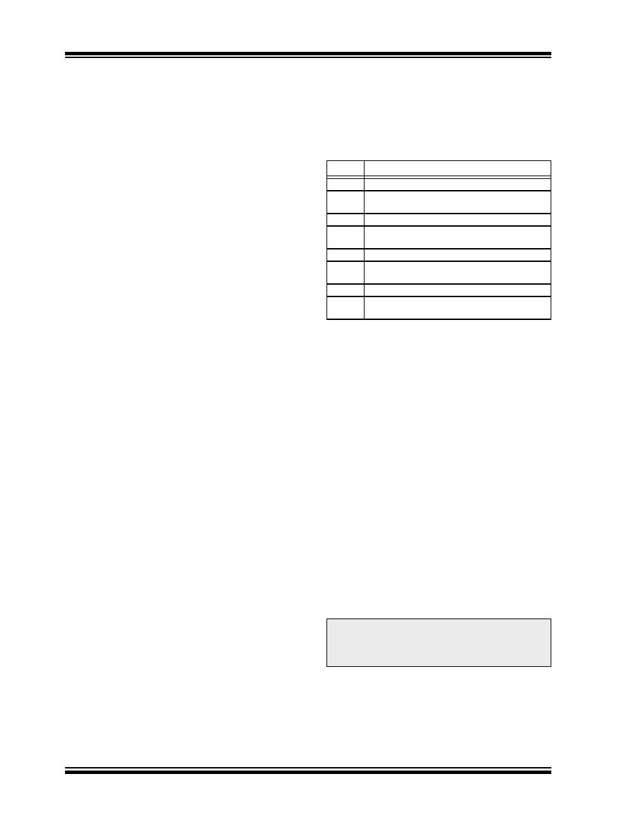
TABLE 15-1:
DEAD-TIME SELECTION BITS
15.7.3
DEAD-TIME RANGES
The amount of dead time provided by each dead-time
unit is selected by specifying the input clock prescaler
value and a 6-bit unsigned value. The amount of dead
time provided by each unit may be set independently.
Four input clock prescaler selections have been pro-
vided to allow a suitable range of dead times, based on
the device operating frequency. The clock prescaler
option may be selected independently for each of the
two dead-time values. The dead-time clock prescaler
values are selected using the DTAPS<1:0> and
DTBPS<1:0> control bits in the DTCON1 SFR. One of
four clock prescaler options (TCY, 2TCY, 4TCY or 8TCY)
may be selected for each of the dead-time values.
After the prescaler values are selected, the dead time
for each unit is adjusted by loading two 6-bit unsigned
values into the DTCON1 SFR.
The dead-time unit prescalers are cleared on the fol-
lowing events:
On a load of the down timer due to a duty cycle
comparison edge event.
On a write to the DTCON1 or DTCON2 registers.
On any device Reset.
Bit
Function
DTS1A
Selects PWM1L/PWM1H active edge dead time.
DTS1I
Selects PWM1L/PWM1H inactive edge
dead time.
DTS2A
Selects PWM2L/PWM2H active edge dead time.
DTS2I
Selects PWM2L/PWM2H inactive edge
dead time.
DTS3A
Selects PWM3L/PWM3H active edge dead time.
DTS3I
Selects PWM3L/PWM3H inactive edge
dead time.
DTS4A
Selects PWM4L/PWM4H active edge dead time.
DTS4I
Selects PWM4L/PWM4H inactive edge
dead time.
Note:
The user should not modify the DTCON1
or DTCON2 values while the PWM mod-
ule is operating (PTEN = 1). Unexpected
results may occur.
相关PDF资料 |
PDF描述 |
|---|---|
| UX60SC-MB-5S8 | CONN RCPT MINI USB2.0 5POS SLD |
| ZX62D-B-5P8 | CONN RCPT MCR USB B SMD TH SHLL |
| AT91SAM7X256B-AU | IC MCU 256KB FLASH 100LQFP |
| ATMEGA165PV-8MU | IC AVR MCU 16K 8MHZ 64-QFN |
| AT32UC3C1256C-AUT | IC MCU AVR32 256K FLASH 100TQFP |
相关代理商/技术参数 |
参数描述 |
|---|---|
| AT32UC3A0256AU-ALUT | 功能描述:32位微控制器 - MCU 256KB Flash Audio 85Deg RoHS:否 制造商:Texas Instruments 核心:C28x 处理器系列:TMS320F28x 数据总线宽度:32 bit 最大时钟频率:90 MHz 程序存储器大小:64 KB 数据 RAM 大小:26 KB 片上 ADC:Yes 工作电源电压:2.97 V to 3.63 V 工作温度范围:- 40 C to + 105 C 封装 / 箱体:LQFP-80 安装风格:SMD/SMT |
| AT32UC3A0256-CTUR | 功能描述:32位微控制器 - MCU 256KB, 144FFBGA Ind RoHS:否 制造商:Texas Instruments 核心:C28x 处理器系列:TMS320F28x 数据总线宽度:32 bit 最大时钟频率:90 MHz 程序存储器大小:64 KB 数据 RAM 大小:26 KB 片上 ADC:Yes 工作电源电压:2.97 V to 3.63 V 工作温度范围:- 40 C to + 105 C 封装 / 箱体:LQFP-80 安装风格:SMD/SMT |
| AT32UC3A0256-CTUT | 功能描述:32位微控制器 - MCU 256KB, 144FFBGA Ind RoHS:否 制造商:Texas Instruments 核心:C28x 处理器系列:TMS320F28x 数据总线宽度:32 bit 最大时钟频率:90 MHz 程序存储器大小:64 KB 数据 RAM 大小:26 KB 片上 ADC:Yes 工作电源电压:2.97 V to 3.63 V 工作温度范围:- 40 C to + 105 C 封装 / 箱体:LQFP-80 安装风格:SMD/SMT |
| AT32UC3A0512 | 制造商:ATMEL 制造商全称:ATMEL Corporation 功能描述:AVR32 32-Bit Microcontroller |
| AT32UC3A0512_08 | 制造商:ATMEL 制造商全称:ATMEL Corporation 功能描述:AVR32 32-Bit Microcontroller |
发布紧急采购,3分钟左右您将得到回复。