- 您现在的位置:买卖IC网 > PDF目录20437 > AT45DB081B-TU (Atmel)IC FLASH 8MBIT 20MHZ 28TSOP PDF资料下载
参数资料
| 型号: | AT45DB081B-TU |
| 厂商: | Atmel |
| 文件页数: | 2/33页 |
| 文件大小: | 0K |
| 描述: | IC FLASH 8MBIT 20MHZ 28TSOP |
| 标准包装: | 234 |
| 格式 - 存储器: | 闪存 |
| 存储器类型: | DataFLASH |
| 存储容量: | 8M(4096 页 x 264 字节) |
| 速度: | 20MHz |
| 接口: | SPI 3 线串行 |
| 电源电压: | 2.7 V ~ 3.6 V |
| 工作温度: | -40°C ~ 85°C |
| 封装/外壳: | 28-TSSOP(0.465",11.8mm 宽) |
| 供应商设备封装: | 28-TSOP |
| 包装: | 托盘 |
第1页当前第2页第3页第4页第5页第6页第7页第8页第9页第10页第11页第12页第13页第14页第15页第16页第17页第18页第19页第20页第21页第22页第23页第24页第25页第26页第27页第28页第29页第30页第31页第32页第33页
�� �
�
�EEPROM� emulation� (bit� or� byte� alterability)� is� easily� handled� with� a� self-contained� three�
�step� Read-Modify-Write� operation.� Unlike� conventional� Flash� memories� that� are�
�accessed� randomly� with� multiple� address� lines� and� a� parallel� interface,� the� DataFlash�
�uses� a� SPI� serial� interface� to� sequentially� access� its� data.� DataFlash� supports� SPI� mode�
�0� and� mode� 3.� The� simple� serial� interface� facilitates� hardware� layout,� increases� system�
�reliability,� minimizes� switching� noise,� and� reduces� package� size� and� active� pin� count.�
�The� device� is� optimized� for� use� in� many� commercial� and� industrial� applications� where�
�high� density,� low� pin� count,� low� voltage,� and� low� power� are� essential.� The� device� oper-�
�ates� at� clock� frequencies� up� to� 20� MHz� with� a� typical� active� read� current� consumption� of�
�4� mA.�
�To� allow� for� simple� in-system� reprogrammability,� the� AT45DB081B� does� not� require�
�high� input� voltages� for� programming.� The� device� operates� from� a� single� power� supply,�
�2.5V� to� 3.6V� or� 2.7V� to� 3.6V,� for� both� the� program� and� read� operations.� The�
�AT45DB081B� is� enabled� through� the� chip� select� pin� (CS)� and� accessed� via� a� three-wire�
�interface� consisting� of� the� Serial� Input� (SI),� Serial� Output� (SO),� and� the� Serial� Clock�
�(SCK).�
�All� programming� cycles� are� self-timed,� and� no� separate� erase� cycle� is� required� before�
�programming.�
�When� the� device� is� shipped� from� Atmel,� the� most� significant� page� of� the� memory� array�
�may� not� be� erased.� In� other� words,� the� contents� of� the� last� page� may� not� be� filled� with�
�FFH.�
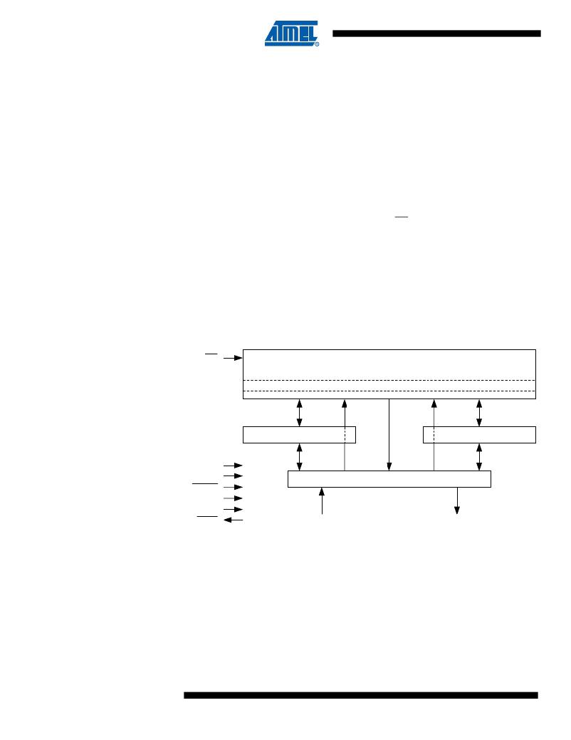
�Block� Diagram�
�WP�
�PAGE� (264� BYTES)�
�FLASH� MEMORY� ARRAY�
�SCK�
�CS�
�RESET�
�VCC�
�GND�
�BUFFER� 1� (264� BYTES)�
�I/O� INTERFACE�
�BUFFER� 2� (264� BYTES)�
�RDY/BUSY�
�SI�
�SO�
�Memory� Array�
�To� provide� optimal� flexibility,� the� memory� array� of� the� AT45DB081B� is� divided� into� three�
�levels� of� granularity� comprising� of� sectors,� blocks,� and� pages.� The� Memory� Architecture�
�Diagram� illustrates� the� breakdown� of� each� level� and� details� the� number� of� pages� per�
�sector� and� block.� All� program� operations� to� the� DataFlash� occur� on� a� page-by-page�
�basis;� however,� the� optional� erase� operations� can� be� performed� at� the� block� or� page�
�level.�
�2�
�AT45DB081B�
�2225J–DFLSH–2/08�
�相关PDF资料 |
PDF描述 |
|---|---|
| T95D277K004CZAS | CAP TANT 270UF 4V 10% 2917 |
| 395-072-527-204 | CARD EDGE 72POS DL .100X.200 BLK |
| ASPI-0412S-1R2N-T3 | INDUCTOR POWER MINI 1.2UH 0412 |
| T95D157M016EZSL | CAP TANT 150UF 16V 20% 2917 |
| 395-072-527-202 | CARD EDGE 72POS DL .100X.200 BLK |
相关代理商/技术参数 |
参数描述 |
|---|---|
| AT45DB081D | 制造商:ATMEL 制造商全称:ATMEL Corporation 功能描述:8-megabit 2.5-volt or 2.7-volt DataFlash |
| AT45DB081D_07 | 制造商:ATMEL 制造商全称:ATMEL Corporation 功能描述:8-megabit 2.5-volt or 2.7-volt DataFlash |
| AT45DB081D_08 | 制造商:ATMEL 制造商全称:ATMEL Corporation 功能描述:8-megabit 2.5-volt or 2.7-volt DataFlash |
| AT45DB081D_09 | 制造商:ATMEL 制造商全称:ATMEL Corporation 功能描述:8-megabit 2.5-volt or 2.7-volt DataFlash |
| AT45DB081D_13 | 制造商:AD 制造商全称:Analog Devices 功能描述:8-megabit 2.5V or 2.7V DataFlash |
发布紧急采购,3分钟左右您将得到回复。