- 您现在的位置:买卖IC网 > PDF目录381463 > AT49BV8192AT (Atmel Corp.) 8-Megabit 1M x 8/ 512K x 16 CMOS Flash Memory PDF资料下载
参数资料
| 型号: | AT49BV8192AT |
| 厂商: | Atmel Corp. |
| 英文描述: | 8-Megabit 1M x 8/ 512K x 16 CMOS Flash Memory |
| 中文描述: | 8兆100万× 8 /为512k × 16的CMOS闪存 |
| 文件页数: | 3/16页 |
| 文件大小: | 246K |
| 代理商: | AT49BV8192AT |
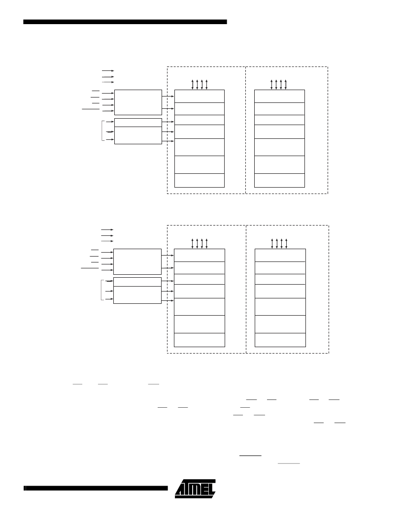
AT49BV008A(T)/8192A(T)
3
AT49BV008A(T) Block Diagram
AT49BV8192A(T) Block Diagram
Device Operation
READ:
The AT49BV008A(T)/8192A(T) is accessed like an
EPROM. When CE and OE are low and WE is high, the
data stored at the memory location determined by the
address pins is asserted on the outputs. The outputs are
put in the high impedance state whenever CE or OE is
high. This dual-line control gives designers flexibility in pre-
venting bus contention.
COMMAND SEQUENCES:
When the device is first pow-
ered on it will be reset to the read or standby mode
depending upon the state of the control line inputs. In order
to perform other device functions, a series of command
sequences are entered into the device. The command
sequences are shown in the Command Definitions table
(I/O8 - I/O15 are don't care inputs for the command codes).
The command sequences are written by applying a low
pulse on the WE or CE input with CE or WE low (respec-
tively) and OE high. The address is latched on the falling
edge of CE or WE, whichever occurs last. The data is
latched by the first rising edge of CE or WE. Standard
microprocessor write timings are used. The address loca-
tions used in the command sequences are not affected by
entering the command sequences.
RESET:
A RESET input pin is provided to ease some sys-
tem applications. When RESET is at a logic high level, the
V
PP
GND
V
CC
OE
WE
CE
CONTROL
LOGIC
DATA INPUTS/OUTPUTS
I/O0 - I/O7
DATA INPUTS/OUTPUTS
I/O0 - I/O7
RESET
ADDRESS
INPUTS
Y DECODER
INPUT/OUTPUT
BUFFERS
PROGRAM DATA
LATCHES
INPUT/OUTPUT
BUFFERS
PROGRAM DATA
LATCHES
Y-GATING
AT49BV008A
AT49BV008AT
Y-GATING
FFFFF
FFFFF
MAIN MEMORY
(992K BYTES)
BOOT BLOCK
16K BYTES
PARAMETER
BLOCK 2
8K BYTES
PARAMETER
BLOCK 1
8K BYTES
PARAMETER
BLOCK 1
8K BYTES
PARAMETER
BLOCK 2
8K BYTES
BOOT BLOCK
16K BYTES
MAIN MEMORY
(992K BYTES)
08000
07FFF
FC000
FBFFF
06000
05FFF
7A000
79FFF
X DECODER
04000
03FFF
78000
77FFF
00000
00000
V
PP
GND
V
CC
OE
WE
CE
CONTROL
LOGIC
DATA INPUTS/OUTPUTS
I/O0 - I/O15
DATA INPUTS/OUTPUTS
I/O0 - I/O15
RESET
ADDRESS
INPUTS
Y DECODER
INPUT/OUTPUT
BUFFERS
PROGRAM DATA
LATCHES
INPUT/OUTPUT
BUFFERS
PROGRAM DATA
LATCHES
Y-GATING
AT49BV8192A
AT49BV8192AT
Y-GATING
7FFFF
7FFFF
MAIN MEMORY
(496K WORDS)
BOOT BLOCK
8K WORDS
PARAMETER
BLOCK 2
4K WORDS
PARAMETER
BLOCK 1
4K WORDS
PARAMETER
BLOCK 1
4K WORDS
PARAMETER
BLOCK 2
4K WORDS
BOOT BLOCK
8K WORDS
MAIN MEMORY
(496K WORDS)
04000
03FFF
7E000
7DFFF
03000
02FFF
7D000
7CFFF
X DECODER
02000
01FFF
7C000
7BFFF
00000
00000
相关PDF资料 |
PDF描述 |
|---|---|
| AT49BV8192AT-12CC | 8-Megabit 1M x 8/ 512K x 16 CMOS Flash Memory |
| AT49BV8192AT-12CI | 8-Megabit 1M x 8/ 512K x 16 CMOS Flash Memory |
| AT49BV8192AT-12TC | 8-Megabit 1M x 8/ 512K x 16 CMOS Flash Memory |
| AT49BV8192AT-12TI | 8-Megabit 1M x 8/ 512K x 16 CMOS Flash Memory |
| AT49BV8192AT-15CC | 8-Megabit 1M x 8/ 512K x 16 CMOS Flash Memory |
相关代理商/技术参数 |
参数描述 |
|---|---|
| AT49BV8192AT-11CC | 制造商:未知厂家 制造商全称:未知厂家 功能描述:x8/x16 Flash EEPROM |
| AT49BV8192AT-11CI | 功能描述:IC FLASH 8MBIT 110NS 48CBGA RoHS:否 类别:集成电路 (IC) >> 存储器 系列:- 标准包装:378 系列:- 格式 - 存储器:闪存 存储器类型:FLASH 存储容量:8M(1M x 8,512K x 16) 速度:110ns 接口:并联 电源电压:2.7 V ~ 3.6 V 工作温度:-40°C ~ 85°C 封装/外壳:48-CBGA 供应商设备封装:48-CBGA(7x7) 包装:托盘 |
| AT49BV8192AT-11TC | 功能描述:IC FLASH 8MBIT 110NS 48TSOP 制造商:microchip technology 系列:- 包装:托盘 零件状态:停產 存储器类型:非易失 存储器格式:闪存 技术:FLASH 存储容量:8Mb (1M x 8,512K x 16) 写周期时间 - 字,页:30μs 访问时间:110ns 存储器接口:并联 电压 - 电源:2.7 V ~ 3.6 V 工作温度:0°C ~ 70°C(TC) 安装类型:表面贴装 封装/外壳:48-TFSOP(0.724",18.40mm 宽) 供应商器件封装:48-TSOP 基本零件编号:AT49BV8192 标准包装:96 |
| AT49BV8192AT-11TI | 制造商:未知厂家 制造商全称:未知厂家 功能描述:EEPROM|FLASH|512KX16/1MX8|CMOS|TSSOP|48PIN|PLASTIC |
| AT49BV8192AT-12CC | 制造商:ATMEL 制造商全称:ATMEL Corporation 功能描述:8-Megabit 1M x 8/ 512K x 16 CMOS Flash Memory |
发布紧急采购,3分钟左右您将得到回复。