参数资料
| 型号: | AT89C51AC3-SLSIM |
| 厂商: | Atmel |
| 文件页数: | 108/140页 |
| 文件大小: | 0K |
| 描述: | IC 8051 MCU FLASH 64K 44PLCC |
| 标准包装: | 27 |
| 系列: | 89C |
| 核心处理器: | 8051 |
| 芯体尺寸: | 8-位 |
| 速度: | 60MHz |
| 连通性: | UART/USART |
| 外围设备: | POR,PWM,WDT |
| 输入/输出数: | 36 |
| 程序存储器容量: | 64KB(64K x 8) |
| 程序存储器类型: | 闪存 |
| EEPROM 大小: | 2K x 8 |
| RAM 容量: | 2.25K x 8 |
| 电压 - 电源 (Vcc/Vdd): | 3 V ~ 5.5 V |
| 数据转换器: | A/D 8x10b |
| 振荡器型: | 外部 |
| 工作温度: | -40°C ~ 85°C |
| 封装/外壳: | 44-LCC(J 形引线) |
| 包装: | 管件 |
第1页第2页第3页第4页第5页第6页第7页第8页第9页第10页第11页第12页第13页第14页第15页第16页第17页第18页第19页第20页第21页第22页第23页第24页第25页第26页第27页第28页第29页第30页第31页第32页第33页第34页第35页第36页第37页第38页第39页第40页第41页第42页第43页第44页第45页第46页第47页第48页第49页第50页第51页第52页第53页第54页第55页第56页第57页第58页第59页第60页第61页第62页第63页第64页第65页第66页第67页第68页第69页第70页第71页第72页第73页第74页第75页第76页第77页第78页第79页第80页第81页第82页第83页第84页第85页第86页第87页第88页第89页第90页第91页第92页第93页第94页第95页第96页第97页第98页第99页第100页第101页第102页第103页第104页第105页第106页第107页当前第108页第109页第110页第111页第112页第113页第114页第115页第116页第117页第118页第119页第120页第121页第122页第123页第124页第125页第126页第127页第128页第129页第130页第131页第132页第133页第134页第135页第136页第137页第138页第139页第140页
7
AT89C51AC3
4383D–8051–02/08
I/O Configurations
Each Port SFR operates via type-D latches, as illustrated in Figure 1 for Ports 3 and 4. A
CPU "write to latch" signal initiates transfer of internal bus data into the type-D latch. A
CPU "read latch" signal transfers the latched Q output onto the internal bus. Similarly, a
"read pin" signal transfers the logical level of the Port pin. Some Port data instructions
activate the "read latch" signal while others activate the "read pin" signal. Latch instruc-
tions are referred to as Read-Modify-Write instructions. Each I/O line may be
independently programmed as input or output.
Port 1, Port 3 and Port 4
Figure 1 shows the structure of Ports 1 and 3, which have internal pull-ups. An external
source can pull the pin low. Each Port pin can be configured either for general-purpose
I/O or for its alternate input output function.
To use a pin for general-purpose output, set or clear the corresponding bit in the Px reg-
ister (x = 1,3 or 4). To use a pin for general-purpose input, set the bit in the Px register.
This turns off the output FET drive.
To configure a pin for its alternate function, set the bit in the Px register. When the latch
is set, the "alternate output function" signal controls the output level (see Figure 1). The
operation of Ports 1, 3 and 4 is discussed further in the "quasi-Bidirectional Port Opera-
tion" section.
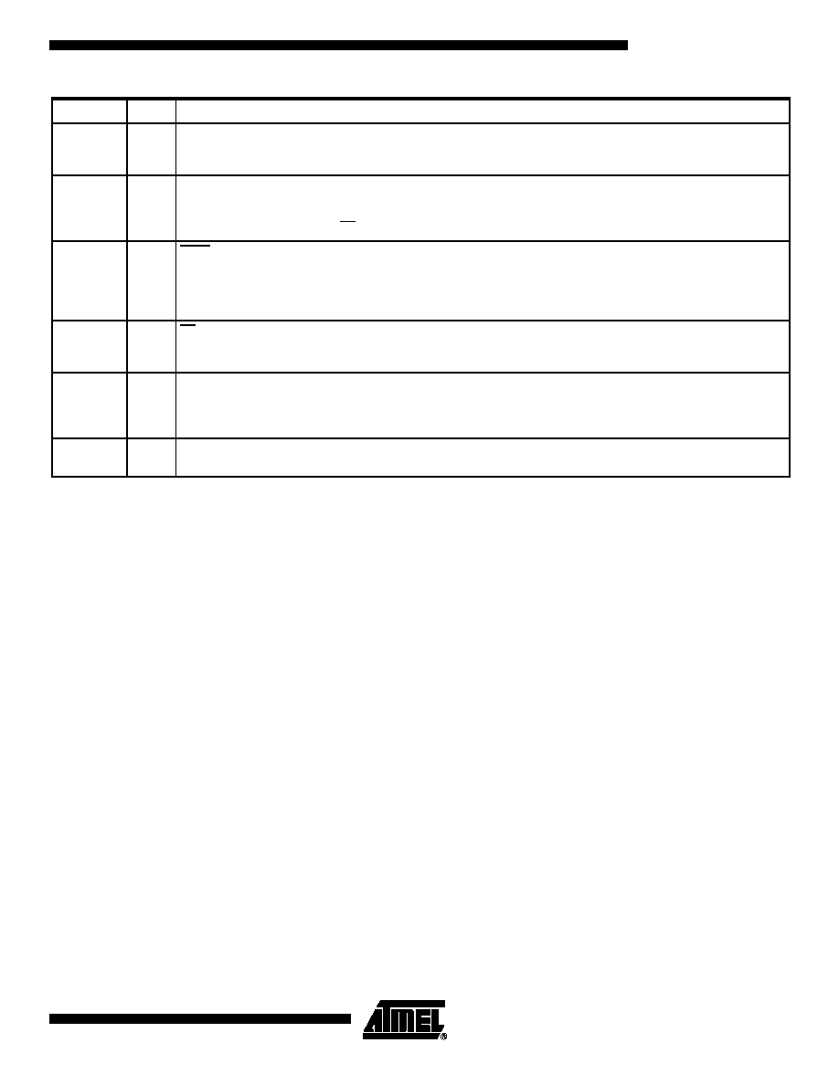
RESET
I/O
Reset:
A high level on this pin during two machine cycles while the oscillator is running resets the device. An internal pull-down
resistor to VSS permits power-on reset using only an external capacitor to VCC.
ALE
O
ALE:
An Address Latch Enable output for latching the low byte of the address during accesses to the external memory. The ALE is
activated every 1/6 oscillator periods (1/3 in X2 mode) except during an external data memory access. When instructions are
executed from an internal Flash (EA = 1), ALE generation can be disabled by the software.
PSEN
O
PSEN:
The Program Store Enable output is a control signal that enables the external program memory of the bus during external
fetch operations. It is activated twice each machine cycle during fetches from the external program memory. However, when
executing from of the external program memory two activations of PSEN are skipped during each access to the external Data
memory. The PSEN is not activated for internal fetches.
EA
I
EA:
When External Access is held at the high level, instructions are fetched from the internal Flash. When held at the low level,
AT89C51AC3 fetches all instructions from the external program memory
.
XTAL1
I
XTAL1:
Input of the inverting oscillator amplifier and input of the internal clock generator circuits.
To drive the device from an external clock source, XTAL1 should be driven, while XTAL2 is left unconnected. To operate
above a frequency of 16 MHz, a duty cycle of 50% should be maintained.
XTAL2
O
XTAL2:
Output from the inverting oscillator amplifier.
Pin Name
Type
Description
相关PDF资料 |
PDF描述 |
|---|---|
| AT89C51CC03C-RLRIM | IC 8051 MCU FLASH 64K 44VQFP |
| AT89C51ED2-SMRUM | IC MCU FLASH 8051 64K 5V 68PLCC |
| AT89C51IC2-RLRUM | IC 8051 MCU 32K FLASH 44-VQFP |
| AT89C51ID2-RLRIM | IC MCU FLASH 8051 64K 5V 44-VQFP |
| AT89C51RC-24PU | IC MCU 32K FLASH 24MHZ 40-DIP |
相关代理商/技术参数 |
参数描述 |
|---|---|
| AT89C51AC3-SLSUM | 功能描述:8位微控制器 -MCU C51AC3 64K FLASHADC EEP 5V RoHS:否 制造商:Silicon Labs 核心:8051 处理器系列:C8051F39x 数据总线宽度:8 bit 最大时钟频率:50 MHz 程序存储器大小:16 KB 数据 RAM 大小:1 KB 片上 ADC:Yes 工作电源电压:1.8 V to 3.6 V 工作温度范围:- 40 C to + 105 C 封装 / 箱体:QFN-20 安装风格:SMD/SMT |
| AT89C51CAEAI-TISUM | 制造商:Atmel Corporation 功能描述: |
| AT89C51CC01 | 制造商:ATMEL 制造商全称:ATMEL Corporation 功能描述:Enhanced 8-bit Microcontroller with CAN Controller and Flash Memory |
| AT89C51CC01CA-RLTUM | 功能描述:8位微控制器 -MCU CAN Bootloader CAN RoHS:否 制造商:Silicon Labs 核心:8051 处理器系列:C8051F39x 数据总线宽度:8 bit 最大时钟频率:50 MHz 程序存储器大小:16 KB 数据 RAM 大小:1 KB 片上 ADC:Yes 工作电源电压:1.8 V to 3.6 V 工作温度范围:- 40 C to + 105 C 封装 / 箱体:QFN-20 安装风格:SMD/SMT |
| AT89C51CC01CA-SLSUM | 功能描述:8位微控制器 -MCU Bootloader CAN RoHS:否 制造商:Silicon Labs 核心:8051 处理器系列:C8051F39x 数据总线宽度:8 bit 最大时钟频率:50 MHz 程序存储器大小:16 KB 数据 RAM 大小:1 KB 片上 ADC:Yes 工作电源电压:1.8 V to 3.6 V 工作温度范围:- 40 C to + 105 C 封装 / 箱体:QFN-20 安装风格:SMD/SMT |
发布紧急采购,3分钟左右您将得到回复。