- 您现在的位置:买卖IC网 > PDF目录12043 > AT89C51RD2-SLRUM (Atmel)IC MCU FLASH 8051 EEP 64K 44PLCC PDF资料下载
参数资料
| 型号: | AT89C51RD2-SLRUM |
| 厂商: | Atmel |
| 文件页数: | 55/137页 |
| 文件大小: | 0K |
| 描述: | IC MCU FLASH 8051 EEP 64K 44PLCC |
| 产品培训模块: | MCU Product Line Introduction |
| 标准包装: | 1 |
| 系列: | 89C |
| 核心处理器: | 8051 |
| 芯体尺寸: | 8-位 |
| 速度: | 60MHz |
| 连通性: | SPI,UART/USART |
| 外围设备: | POR,PWM,WDT |
| 输入/输出数: | 34 |
| 程序存储器容量: | 64KB(64K x 8) |
| 程序存储器类型: | 闪存 |
| RAM 容量: | 2K x 8 |
| 电压 - 电源 (Vcc/Vdd): | 2.7 V ~ 5.5 V |
| 振荡器型: | 外部 |
| 工作温度: | -40°C ~ 85°C |
| 封装/外壳: | 44-LCC(J 形引线) |
| 包装: | 标准包装 |
| 配用: | AT89OCD-01-ND - USB EMULATOR FOR AT8XC51 MCU AT89STK-11-ND - KIT STARTER FOR AT89C51RX2 |
| 其它名称: | AT89C51RD2-SLRUMDKR |
第1页第2页第3页第4页第5页第6页第7页第8页第9页第10页第11页第12页第13页第14页第15页第16页第17页第18页第19页第20页第21页第22页第23页第24页第25页第26页第27页第28页第29页第30页第31页第32页第33页第34页第35页第36页第37页第38页第39页第40页第41页第42页第43页第44页第45页第46页第47页第48页第49页第50页第51页第52页第53页第54页当前第55页第56页第57页第58页第59页第60页第61页第62页第63页第64页第65页第66页第67页第68页第69页第70页第71页第72页第73页第74页第75页第76页第77页第78页第79页第80页第81页第82页第83页第84页第85页第86页第87页第88页第89页第90页第91页第92页第93页第94页第95页第96页第97页第98页第99页第100页第101页第102页第103页第104页第105页第106页第107页第108页第109页第110页第111页第112页第113页第114页第115页第116页第117页第118页第119页第120页第121页第122页第123页第124页第125页第126页第127页第128页第129页第130页第131页第132页第133页第134页第135页第136页第137页
24
4235K–8051–05/08
AT89C51RD2/ED2
part of the available XRAM as explained in Table 9-1. This can be useful if external
peripherals are mapped at addresses already used by the internal XRAM.
With EXTRAM = 0, the XRAM is indirectly addressed, using the MOVX instruction in
combination with any of the registers R0, R1 of the selected bank or DPTR. An access to
XRAM will not affect ports P0, P2, P3.6 (WR) and P3.7 (RD). For example, with EXTRAM =
0, MOVX @R0, # data where R0 contains 0A0H, accesses the XRAM at address 0A0H
rather than external memory. An access to external data memory locations higher than the
accessible size of the XRAM will be performed with the MOVX DPTR instructions in the same
way as in the standard 80C51, with P0 and P2 as data/address busses, and P3.6 and P3.7
as write and read timing signals. Accesses to XRAM above 0FFH can only be done by the
use of DPTR.
With EXTRAM = 1, MOVX @Ri and MOVX @DPTR will be similar to the standard
80C51.MOVX @ Ri will provide an eight-bit address multiplexed with data on Port0 and any
output port pins can be used to output higher order address bits. This is to provide the
external paging capability. MOVX @DPTR will generate a sixteen-bit address. Port2 outputs
the high-order eight address bits (the contents of DPH) while Port0 multiplexes the low-order
eight address bits (DPL) with data. MOVX @ Ri and MOVX @DPTR will generate either read
or write signals on P3.6 (WR) and P3.7 (RD).
The stack pointer (SP) may be located anywhere in the 256 bytes RAM (lower and upper RAM)
internal data memory. The stack may not be located in the XRAM.
The M0 bit allows to stretch the XRAM timings; if M0 is set, the read and write pulses are
extended from 6 to 30 clock periods. This is useful to access external slow peripherals.
9.1
Registers
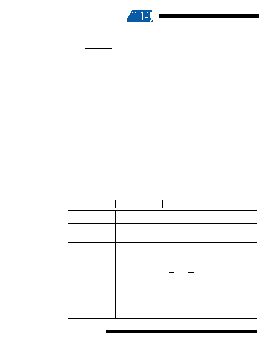
Table 9-1.
AUXR Register
AUXR - Auxiliary Register (8Eh)
7
6
5
4
3
2
1
0
DPU
-
M0
XRS2
XRS1
XRS0
EXTRAM
AO
Bit
Number
Bit
Mnemonic
Description
7
DPU
Disable Weak Pull-up
Cleared by software to activate the permanent weak pull-up (default)
Set by software to disable the weak pull-up (reduce power consumption)
6
-
Reserved
The value read from this bit is indeterminate. Do not set this bit.
5
M0
Pulse length
Cleared to stretch MOVX control: the RD and the WR pulse length is 6 clock periods
(default).
Set to stretch MOVX control: the RD and the WR pulse length is 30 clock periods.
4
XRS2
XRAM Size
XRS2XRS1XRS0XRAM size
0
0256 bytes
0
1
512 bytes
0
1
0768 bytes(default)
0
1
11024 bytes
1
0
01792 bytes
3
XRS1
2
XRS0
相关PDF资料 |
PDF描述 |
|---|---|
| VE-23V-IY-F2 | CONVERTER MOD DC/DC 5.8V 50W |
| VE-23V-IY-F1 | CONVERTER MOD DC/DC 5.8V 50W |
| D-621-0424 | CONN JACK TRIAXIAL W/SOCKET |
| 5221629-6 | CONN TERMINATR PLUG BNC 93OHM AU |
| VE-23T-IY-F2 | CONVERTER MOD DC/DC 6.5V 50W |
相关代理商/技术参数 |
参数描述 |
|---|---|
| AT89C51RD2-SLSIM | 功能描述:IC 8051 MCU FLASH 64K 44PLCC RoHS:否 类别:集成电路 (IC) >> 嵌入式 - 微控制器, 系列:89C 标准包装:9 系列:87C 核心处理器:8051 芯体尺寸:8-位 速度:40/20MHz 连通性:UART/USART 外围设备:POR,WDT 输入/输出数:32 程序存储器容量:32KB(32K x 8) 程序存储器类型:OTP EEPROM 大小:- RAM 容量:256 x 8 电压 - 电源 (Vcc/Vdd):4.5 V ~ 5.5 V 数据转换器:- 振荡器型:内部 工作温度:0°C ~ 70°C 封装/外壳:40-DIP(0.600",15.24mm) 包装:管件 |
| AT89C51RD2-SLSUM | 功能描述:8位微控制器 -MCU 64kB Flash 2048B RAM 2.7V-5.5V RoHS:否 制造商:Silicon Labs 核心:8051 处理器系列:C8051F39x 数据总线宽度:8 bit 最大时钟频率:50 MHz 程序存储器大小:16 KB 数据 RAM 大小:1 KB 片上 ADC:Yes 工作电源电压:1.8 V to 3.6 V 工作温度范围:- 40 C to + 105 C 封装 / 箱体:QFN-20 安装风格:SMD/SMT |
| AT89C51RD2-SLSUM | 制造商:Atmel Corporation 功能描述:IC 8BIT MCU C51/C251 60MHZ 44-PLCC |
| AT89C51RD2-SMSIM | 制造商:ATMEL 制造商全称:ATMEL Corporation 功能描述:8-bit Flash Microcontroller |
| AT89C51RD2-SMSUM | 制造商:ATMEL 制造商全称:ATMEL Corporation 功能描述:8-bit Flash Microcontroller |
发布紧急采购,3分钟左右您将得到回复。