- 您现在的位置:买卖IC网 > PDF目录11214 > AT89LP828-20JU (Atmel)MCU 8051 8K FLASH SPI 32PLCC PDF资料下载
参数资料
| 型号: | AT89LP828-20JU |
| 厂商: | Atmel |
| 文件页数: | 70/149页 |
| 文件大小: | 0K |
| 描述: | MCU 8051 8K FLASH SPI 32PLCC |
| 产品培训模块: | MCU Product Line Introduction |
| 标准包装: | 32 |
| 系列: | 89LP |
| 核心处理器: | 8051 |
| 芯体尺寸: | 8-位 |
| 速度: | 20MHz |
| 连通性: | SPI,UART/USART |
| 外围设备: | 欠压检测/复位,POR,PWM,WDT |
| 输入/输出数: | 30 |
| 程序存储器容量: | 8KB(8K x 8) |
| 程序存储器类型: | 闪存 |
| EEPROM 大小: | 1K x 8 |
| RAM 容量: | 768 x 8 |
| 电压 - 电源 (Vcc/Vdd): | 2.4 V ~ 5.5 V |
| 振荡器型: | 内部 |
| 工作温度: | -40°C ~ 85°C |
| 封装/外壳: | 32-LCC(J 形引线) |
| 包装: | 管件 |
第1页第2页第3页第4页第5页第6页第7页第8页第9页第10页第11页第12页第13页第14页第15页第16页第17页第18页第19页第20页第21页第22页第23页第24页第25页第26页第27页第28页第29页第30页第31页第32页第33页第34页第35页第36页第37页第38页第39页第40页第41页第42页第43页第44页第45页第46页第47页第48页第49页第50页第51页第52页第53页第54页第55页第56页第57页第58页第59页第60页第61页第62页第63页第64页第65页第66页第67页第68页第69页当前第70页第71页第72页第73页第74页第75页第76页第77页第78页第79页第80页第81页第82页第83页第84页第85页第86页第87页第88页第89页第90页第91页第92页第93页第94页第95页第96页第97页第98页第99页第100页第101页第102页第103页第104页第105页第106页第107页第108页第109页第110页第111页第112页第113页第114页第115页第116页第117页第118页第119页第120页第121页第122页第123页第124页第125页第126页第127页第128页第129页第130页第131页第132页第133页第134页第135页第136页第137页第138页第139页第140页第141页第142页第143页第144页第145页第146页第147页第148页第149页
27
3654A–MICRO–8/09
AT89LP428/828
8.2
Power-down Mode
Setting the Power-down (PD) bit in PCON enters Power-down mode. Power-down mode stops
the oscillator, disables the BOD and powers down the Flash memory in order to minimize power
consumption. Only the power-on circuitry will continue to draw power during Power-down. Dur-
ing Power-down, the power supply voltage may be reduced to the RAM keep-alive voltage. The
RAM contents will be retained, but the SFR contents are not guaranteed once V
CC has been
reduced. Power-down may be exited by external reset, power-on reset, or certain enabled
interrupts.
8.2.1
Interrupt Recovery from Power-down
Three external interrupt sources may be configured to terminate Power-down mode: external
interrupts INT0 (P3.2) and INT1 (P3.3); and the GPI. To wake up by external interrupt INT0 or
INT1, that interrupt must be enabled by setting EX0 or EX1 in IE and must be configured for
level-sensitive operation by clearing IT0 or IT1. Any GPI on Port 1 (GPI
7-0) can also wake up the
device. The GPI pin must be enabled in GPIEN and configured for level-sensitive detection, and
EGP in IE2 must be set in order to terminate Power-down.
When terminating Power-down by an interrupt, two different wake-up modes are available.
When PWDEX in PCON is zero, the wake-up period is internally timed as shown in Figure 8-1.
At the falling edge on the interrupt pin, Power-down is exited, the oscillator is restarted, and an
internal timer begins counting. The internal clock will not be allowed to propagate to the CPU
until after the timer has timed out. After the time-out period, the interrupt service routine will
begin. The time-out period is controlled by the Start-up Timer Fuses (see Table 7-1 on page 25).
The interrupt pin need not remain low for the entire time-out period.
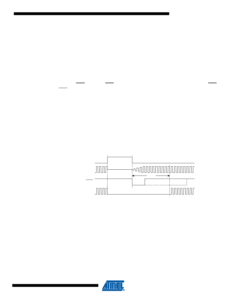
Figure 8-1.
Interrupt Recovery from Power-down (PWDEX = 0)
When PWDEX = “1”, the wake-up period is controlled externally by the interrupt. Again, at
the falling edge on the interrupt pin, power-down is exited and the oscillator is restarted. How-
ever, the internal clock will not propagate until the rising edge of the interrupt pin as shown in
Figure 8-2. The interrupt pin should be held low long enough for the selected clock source to sta-
bilize. After the rising edge on the pin the interrupt service routine will be executed.
PWD
INT1
XTAL1
tSUT
Internal
Clock
相关PDF资料 |
PDF描述 |
|---|---|
| VI-B21-IX-F4 | CONVERTER MOD DC/DC 12V 75W |
| VI-B21-IX-F3 | CONVERTER MOD DC/DC 12V 75W |
| VI-B21-IX-F1 | CONVERTER MOD DC/DC 12V 75W |
| ADG508FBRN | IC MULTIPLEXER 8X1 16SOIC |
| VI-B21-IW-F4 | CONVERTER MOD DC/DC 12V 100W |
相关代理商/技术参数 |
参数描述 |
|---|---|
| AT89LP828-20MH | 功能描述:8位微控制器 -MCU Single Cycle 8051 8K ISP Flash 2.4V-5.5V RoHS:否 制造商:Silicon Labs 核心:8051 处理器系列:C8051F39x 数据总线宽度:8 bit 最大时钟频率:50 MHz 程序存储器大小:16 KB 数据 RAM 大小:1 KB 片上 ADC:Yes 工作电源电压:1.8 V to 3.6 V 工作温度范围:- 40 C to + 105 C 封装 / 箱体:QFN-20 安装风格:SMD/SMT |
| AT89LP828-20PU | 功能描述:8位微控制器 -MCU Single Cycle 8051 8K ISP Flash 2.4V-5.5V RoHS:否 制造商:Silicon Labs 核心:8051 处理器系列:C8051F39x 数据总线宽度:8 bit 最大时钟频率:50 MHz 程序存储器大小:16 KB 数据 RAM 大小:1 KB 片上 ADC:Yes 工作电源电压:1.8 V to 3.6 V 工作温度范围:- 40 C to + 105 C 封装 / 箱体:QFN-20 安装风格:SMD/SMT |
| AT89LP828-AU | 功能描述:8位微控制器 -MCU Single-Cycle 8051 8K ISP Flash, 2.4-5.5V RoHS:否 制造商:Silicon Labs 核心:8051 处理器系列:C8051F39x 数据总线宽度:8 bit 最大时钟频率:50 MHz 程序存储器大小:16 KB 数据 RAM 大小:1 KB 片上 ADC:Yes 工作电源电压:1.8 V to 3.6 V 工作温度范围:- 40 C to + 105 C 封装 / 箱体:QFN-20 安装风格:SMD/SMT |
| AT89LP828-JU | 功能描述:8位微控制器 -MCU Single-Cycle 8051 8K ISP Flash, 2.4-5.5V RoHS:否 制造商:Silicon Labs 核心:8051 处理器系列:C8051F39x 数据总线宽度:8 bit 最大时钟频率:50 MHz 程序存储器大小:16 KB 数据 RAM 大小:1 KB 片上 ADC:Yes 工作电源电压:1.8 V to 3.6 V 工作温度范围:- 40 C to + 105 C 封装 / 箱体:QFN-20 安装风格:SMD/SMT |
| AT89LP828-PU | 功能描述:8位微控制器 -MCU Single-Cycle 8051 8K ISP Flash, 2.4-5.5V RoHS:否 制造商:Silicon Labs 核心:8051 处理器系列:C8051F39x 数据总线宽度:8 bit 最大时钟频率:50 MHz 程序存储器大小:16 KB 数据 RAM 大小:1 KB 片上 ADC:Yes 工作电源电压:1.8 V to 3.6 V 工作温度范围:- 40 C to + 105 C 封装 / 箱体:QFN-20 安装风格:SMD/SMT |
发布紧急采购,3分钟左右您将得到回复。