- 您现在的位置:买卖IC网 > PDF目录67389 > ATF-33143-TR1 X BAND, Si, N-CHANNEL, RF SMALL SIGNAL, HEMFET PDF资料下载
参数资料
| 型号: | ATF-33143-TR1 |
| 元件分类: | 小信号晶体管 |
| 英文描述: | X BAND, Si, N-CHANNEL, RF SMALL SIGNAL, HEMFET |
| 封装: | PLASTIC, SC-70, 4 PIN |
| 文件页数: | 11/18页 |
| 文件大小: | 154K |
| 代理商: | ATF-33143-TR1 |
2
ATF-33143 Absolute Maximum Ratings[1]
Absolute
Symbol
Parameter
Units
Maximum
VDS
Drain - Source Voltage [2]
V
5.5
VGS
Gate - Source Voltage [2]
V-5
VGD
Gate Drain Voltage[2]
V-5
IDS
Drain Current[2]
mA
Idss[3]
Pdiss
Total Power Dissipation[4]
mW
600
Pin max
RF Input Power
dBm
20
TCH
Channel Temperature[5]
°C
160
TSTG
Storage Temperature
°C
-65 to 160
θ
jc
Thermal Resistance [6]
°C/W
145
Notes:
1. Operation of this device above any one of
these parameters may cause permanent
damage.
2. Assumes DC quiesent conditions.
3. VGS = 0 V
4. Source lead temperature is 25
°C. Derate
6 mW/
°C for TL > 60°C.
5. Please refer to failure rates in reliability
section to assess the reliability impact of
running devices above a channel tempera-
ture of 140
°C.
6. Thermal resistance measured using 150
°C
Liquid Crystal Measurement method.
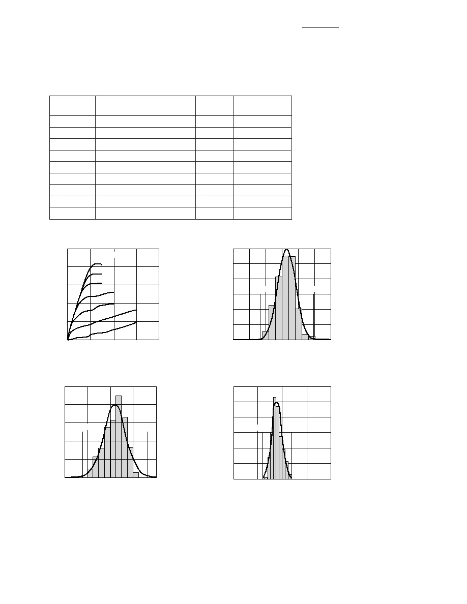
Product Consistency Distribution Charts [8, 9]
VDS (V)
Figure 1. Typical Pulsed I-V Curves[7].
(VGS = -0.2 V per step)
I DS
(mA)
02
4
6
8
500
400
300
200
100
0
0 V
–0.6 V
+0.6 V
NF (dB)
Figure 2. NF @ 2 GHz, 4 V, 80 mA.
LSL=0.2, Nominal=0.53, USL=0.8
0.2
0.4
0.3
0.6
0.5
0.8
0.7
-3 Std
+3 Std
Cpk = 1.7
Std = 0.05
120
100
80
60
40
20
0
OIP3 (dBm)
Figure 3. OIP3 @ 2 GHz, 4 V, 80 mA.
LSL=30.0, Nominal=33.3, USL=37.0
29
37
-3 Std
+3 Std
Cpk = 1.21
Std = 0.94
100
80
60
40
20
0
33
31
35
GAIN (dB)
Figure 4. Gain @ 2 GHz, 4 V, 80 mA.
LSL=13.5, Nominal=14.8, USL=16.5
13
14
15
16
17
-3 Std
+3 Std
Cpk = 2.3
Std = 0.2
120
100
80
60
40
20
0
Notes:
7. Under large signal conditions, VGS may swing
positive and the drain current may exceed
Idss. These conditions are acceptable as long
as the maximum Pdiss and Pin max ratings are
not exceeded.
8. Distribution data sample size is 450 samples
taken from 9 different wafers. Future wafers
allocated to this product may have nominal
values anywhere within the upper and lower
spec limits.
9. Measurements made on production test
board. This circuit represents a trade-off
between an optimal noise match and a
realizeable match based on production test
requirements. Circuit losses have been de-
embedded from actual measurements.
10. The probability of a parameter being
between
±1σ is 68.3%, between ±2σ is
95.4% and between
±3σ is 99.7%.
相关PDF资料 |
PDF描述 |
|---|---|
| ATF-50189 | 0 MHz - 2400 MHz RF/MICROWAVE NARROW BAND MEDIUM POWER AMPLIFIER |
| ATS535SSB | PROXIMITY SENSOR-HALL EFFECT, 65-95mA, ROUND, THROUGH HOLE MOUNT |
| ATS535JSB | PROXIMITY SENSOR-HALL EFFECT, 65-95mA, ROUND, THROUGH HOLE MOUNT |
| ATS611LSB | PROXIMITY SENSOR-HALL EFFECT, 0.5-2.5mm, 0.40V, ROUND, THROUGH HOLE MOUNT |
| ATS660LSB | PROXIMITY SENSOR-HALL EFFECT, 0.5-2.5mm, 0.40V, ROUND, THROUGH HOLE MOUNT |
相关代理商/技术参数 |
参数描述 |
|---|---|
| ATF-33143-TR1G | 功能描述:射频GaAs晶体管 Transistor GaAs Low Noise RoHS:否 制造商:TriQuint Semiconductor 技术类型:pHEMT 频率:500 MHz to 3 GHz 增益:10 dB 噪声系数: 正向跨导 gFS(最大值/最小值):4 S 漏源电压 VDS: 闸/源击穿电压:- 8 V 漏极连续电流:3 A 最大工作温度:+ 150 C 功率耗散:10 W 安装风格: 封装 / 箱体: |
| ATF-33143-TR2 | 制造商:AGILENT 制造商全称:AGILENT 功能描述:Low Noise Pseudomorphic HEMT in a Surface Mount Plastic Package |
| ATF-33143-TR2G | 功能描述:射频GaAs晶体管 Transistor GaAs Low Noise RoHS:否 制造商:TriQuint Semiconductor 技术类型:pHEMT 频率:500 MHz to 3 GHz 增益:10 dB 噪声系数: 正向跨导 gFS(最大值/最小值):4 S 漏源电压 VDS: 闸/源击穿电压:- 8 V 漏极连续电流:3 A 最大工作温度:+ 150 C 功率耗散:10 W 安装风格: 封装 / 箱体: |
| ATF331M4 | 制造商:AGILENT 制造商全称:AGILENT 功能描述:Agilent ATF-331M4 Low Noise Pseudomorphic HEMT in a Miniature Leadless Package |
| ATF-331M4 | 制造商:未知厂家 制造商全称:未知厂家 功能描述:PHEMT Low Noise +31 dBm OIP3 in MiniPak |
发布紧急采购,3分钟左右您将得到回复。