- 您现在的位置:买卖IC网 > PDF目录42901 > ATF-331M4-TR1G (AGILENT TECHNOLOGIES INC) X BAND, Si, N-CHANNEL, RF SMALL SIGNAL, HEMFET PDF资料下载
参数资料
| 型号: | ATF-331M4-TR1G |
| 厂商: | AGILENT TECHNOLOGIES INC |
| 元件分类: | 小信号晶体管 |
| 英文描述: | X BAND, Si, N-CHANNEL, RF SMALL SIGNAL, HEMFET |
| 封装: | MINIPAK-4 |
| 文件页数: | 4/16页 |
| 文件大小: | 212K |
| 代理商: | ATF-331M4-TR1G |
12
TIME (seconds)
T
MAX
TEMPERATURE
(°
C)
0
50
100
150
200
250
60
Preheat
Zone
Cool Down
Zone
Reflow
Zone
120
180
240
300
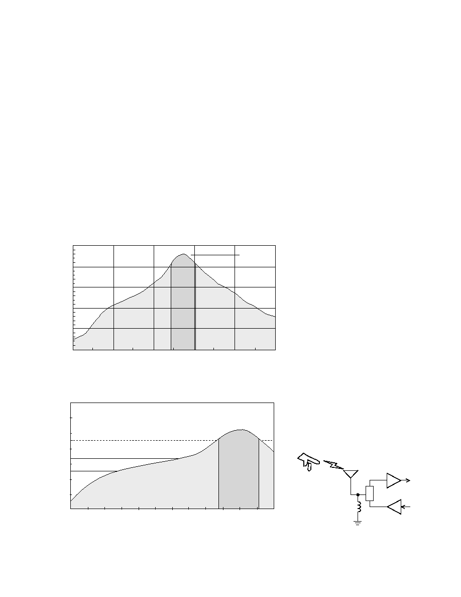
Figure 25. Lead-free Solder Reflow Profile.
Figure 24. Leaded Solder Reflow Profile.
TIME (seconds)
Peak Temperature
Min. 240
°C
Max. 255
°C
TEMPERATURE
(°
C)
0
50
150
100
221
200
250
300
350
60
90
30
120
150
210
180
270
300
330
240
360
Preheat 130 – 170
°C
Min. 60s
Max. 150s
Reflow Time
Min. 60s
Max. 90s
evaporating solvents from the
solder paste. The reflow zone
briefly elevates the temperature
sufficiently to produce a reflow
of the solder.
The rates of change of tempera-
ture for the ramp-up and cool-
down zones are chosen to be low
enough to not cause deformation
of board or damage to compo-
nents due to thermal shock. The
maximum temperature in the
reflow zone (Tmax) should not
exceed 235
°C for leaded solder.
These parameters are typical for
a surface mount assembly
process for the ATF-331M4. As a
general guideline, the circuit
board and components should
only be exposed to the minimum
temperatures and times the
necessary to achieve a uniform
reflow of solder.
The recommended lead-free
reflow profile is shown in
Figure 25.
Electrostatic Sensitivity
FETs and RFICs are electrostatic
discharge (ESD) sensitive de-
vices. Agilent devices are manu-
factured using a very robust and
reliable PHEMT process, however,
permanent damage may occur to
these devices if they are sub-
jected to high-energy electrostatic
discharges. Electrostatic charges
as high as several thousand volts
(which readily accumulate on the
human body and on test equip-
ment) can discharge without
detection and may result in
failure or degradation in perfor-
mance and reliability.
Electronic devices may be
subjected to ESD damage in any
of the following areas:
Storage & handling
Inspection
Assembly & testing
In-circuit use
The ATF-331M4 is an ESD
Class 1 device. Therefore, proper
ESD precautions are recom-
mended when handling, inspect-
ing, testing, and assembling these
devices to avoid damage.
Any user-accessible points in
wireless equipment (e.g. antenna
or battery terminals) provide an
opportunity for ESD damage.
For circuit applications in which
the ATF-331M4 is used as an
input or output stage with close
coupling to an external antenna,
the device should be protected
from high voltage spikes due to
human contact with the antenna.
A good practice, illustrated in
Figure 26, is to place a shunt
inductor or RF choke at the
antenna connection to protect
the receiver and transmitter
circuits. It is often advantageous
to integrate the RF choke into the
design of the diplexer or T/R
switch control circuitry.
Figure 26. In-circuit ESD Protection.
相关PDF资料 |
PDF描述 |
|---|---|
| ATF-331M4-BLKG | X BAND, Si, N-CHANNEL, RF SMALL SIGNAL, HEMFET |
| ATF-34143-TR2G | X BAND, Si, N-CHANNEL, RF SMALL SIGNAL, HEMFET |
| ATF-34143-TR1G | X BAND, Si, N-CHANNEL, RF SMALL SIGNAL, HEMFET |
| ATF-34143-TR1 | X BAND, Si, N-CHANNEL, RF SMALL SIGNAL, HEMFET |
| ATF-34143-BLK | X BAND, Si, N-CHANNEL, RF SMALL SIGNAL, HEMFET |
相关代理商/技术参数 |
参数描述 |
|---|---|
| ATF-331M4-TR2 | 功能描述:射频GaAs晶体管 Transistor GaAs Low Noise RoHS:否 制造商:TriQuint Semiconductor 技术类型:pHEMT 频率:500 MHz to 3 GHz 增益:10 dB 噪声系数: 正向跨导 gFS(最大值/最小值):4 S 漏源电压 VDS: 闸/源击穿电压:- 8 V 漏极连续电流:3 A 最大工作温度:+ 150 C 功率耗散:10 W 安装风格: 封装 / 箱体: |
| ATF34143 | 制造商:HP 制造商全称:Agilent(Hewlett-Packard) 功能描述:Low Noise Pseudomorphic HEMT in a Surface Mount Plastic Package |
| ATF-34143 | 制造商:Avago Technologies 功能描述:MOSFET RF SOT-343 |
| ATF34143BLK | 制造商:未知厂家 制造商全称:未知厂家 功能描述:TRANSISTOR | JFET | N-CHANNEL | 5.5V V(BR)DSS | 90MA I(DSS) | SOT-343R |
| ATF-34143-BLK | 制造商:Agilent Technologies 功能描述:JFET Transistor, N-Channel, SOT-343R |
发布紧急采购,3分钟左右您将得到回复。