- 您现在的位置:买卖IC网 > PDF目录295118 > AX125-1CS180I FPGA, 1344 CLBS, 82000 GATES, 763 MHz, PBGA180 PDF资料下载
参数资料
| 型号: | AX125-1CS180I |
| 元件分类: | FPGA |
| 英文描述: | FPGA, 1344 CLBS, 82000 GATES, 763 MHz, PBGA180 |
| 封装: | 0.80 MM PITCH, CSP-180 |
| 文件页数: | 204/230页 |
| 文件大小: | 6485K |
| 代理商: | AX125-1CS180I |
第1页第2页第3页第4页第5页第6页第7页第8页第9页第10页第11页第12页第13页第14页第15页第16页第17页第18页第19页第20页第21页第22页第23页第24页第25页第26页第27页第28页第29页第30页第31页第32页第33页第34页第35页第36页第37页第38页第39页第40页第41页第42页第43页第44页第45页第46页第47页第48页第49页第50页第51页第52页第53页第54页第55页第56页第57页第58页第59页第60页第61页第62页第63页第64页第65页第66页第67页第68页第69页第70页第71页第72页第73页第74页第75页第76页第77页第78页第79页第80页第81页第82页第83页第84页第85页第86页第87页第88页第89页第90页第91页第92页第93页第94页第95页第96页第97页第98页第99页第100页第101页第102页第103页第104页第105页第106页第107页第108页第109页第110页第111页第112页第113页第114页第115页第116页第117页第118页第119页第120页第121页第122页第123页第124页第125页第126页第127页第128页第129页第130页第131页第132页第133页第134页第135页第136页第137页第138页第139页第140页第141页第142页第143页第144页第145页第146页第147页第148页第149页第150页第151页第152页第153页第154页第155页第156页第157页第158页第159页第160页第161页第162页第163页第164页第165页第166页第167页第168页第169页第170页第171页第172页第173页第174页第175页第176页第177页第178页第179页第180页第181页第182页第183页第184页第185页第186页第187页第188页第189页第190页第191页第192页第193页第194页第195页第196页第197页第198页第199页第200页第201页第202页第203页当前第204页第205页第206页第207页第208页第209页第210页第211页第212页第213页第214页第215页第216页第217页第218页第219页第220页第221页第222页第223页第224页第225页第226页第227页第228页第229页第230页
Axcelerator Family FPGAs
v2.8
2-61
The HM and CM modules can select between:
The HCLK or CLK source respectively
A local signal routed on generic routing resources
This
allows
each
core
tile
to
have
eight
clocks
independent of the other core tiles in the device.
Both HCLK and CLK are segmentable, meaning that
individual branches of the global resource can be used
independently.
Like the HM and CM modules, the HD and RD modules
can select between:
The HCLK or CLK source from the HM or CM
module respectively
A local signal routed on generic routing resources
The AX architecture is capable of supporting a large
number of local clocks – 24 segments per HCLK driving
north-south and 28 segments per CLK driving east-west
per core tile.
Actel's
Designer
software’s
place-and-route
takes
advantage of the segmented clock structure found in
Axcelerator devices by turning off any unused clock
segments. This results in not only better performance but
also lower power consumption.
Global Resource Access Macros
Global resources can be driven by one of three sources:
external pad(s), an internal net, or the output of a PLL.
These connections can be made by using one of three
types of macros: CLKBUF, CLKINT, and PLLCLK.
CLKBUF and HCLKBUF
CLKBUF (HCLKBUF) is used to drive a CLK (HCLK) from
external pads. These macros can be used either
generically or with the specific I/O standard desired
(e.g.
CLKBUF_LVCMOS25,
HCLKBUF_LVDS,
etc.)
(Figure 2-42).
Package pins CLKEP and CLKEN are associated with
CLKE; package pins HCLKAP and HCLKAN are
associated with HCLKA, etc.
Note that when CLKBUF (HCLKBUF) is used with a
single-ended I/O standard, it must be tied to the P-
pad of the CLK (HCLK) package pin. In this case, the
CLK (HCLK) N-pad can be used for user signals.
CLKINT and HCLKINT
CLKINT (HCLKINT) is used to access the CLK (HCLK)
resource internally from the user signals (Figure 2-43).
PLLRCLK and PLLHCLK
PLLRCLK (PLLHCLK) is used to drive global resource
CLK (HCLK) from a PLL (Figure 2-44).
Using Global Resources with PLLs
Each global resource has an associated PLL at its root. For
example, PLLA can drive HCLKA, PLLE can drive CLKE, etc.
In addition, each clock pin of the package can be used to
drive either its associated global resource or PLL. For
example, package pins CLKEP and CLKEN can drive either
the RefCLK input of PLLE or CLKE.
There are two macros required when interfacing the
embedded PLLs with the global resources: PLLINT and PLLOUT.
PLLINT
This macro is used to drive the RefCLK input of the PLL
internally from user signals.
PLLOUT
This macro is used to connect either the CLK1 or CLK2
output of a PLL to the regular routing network (Figure 2-
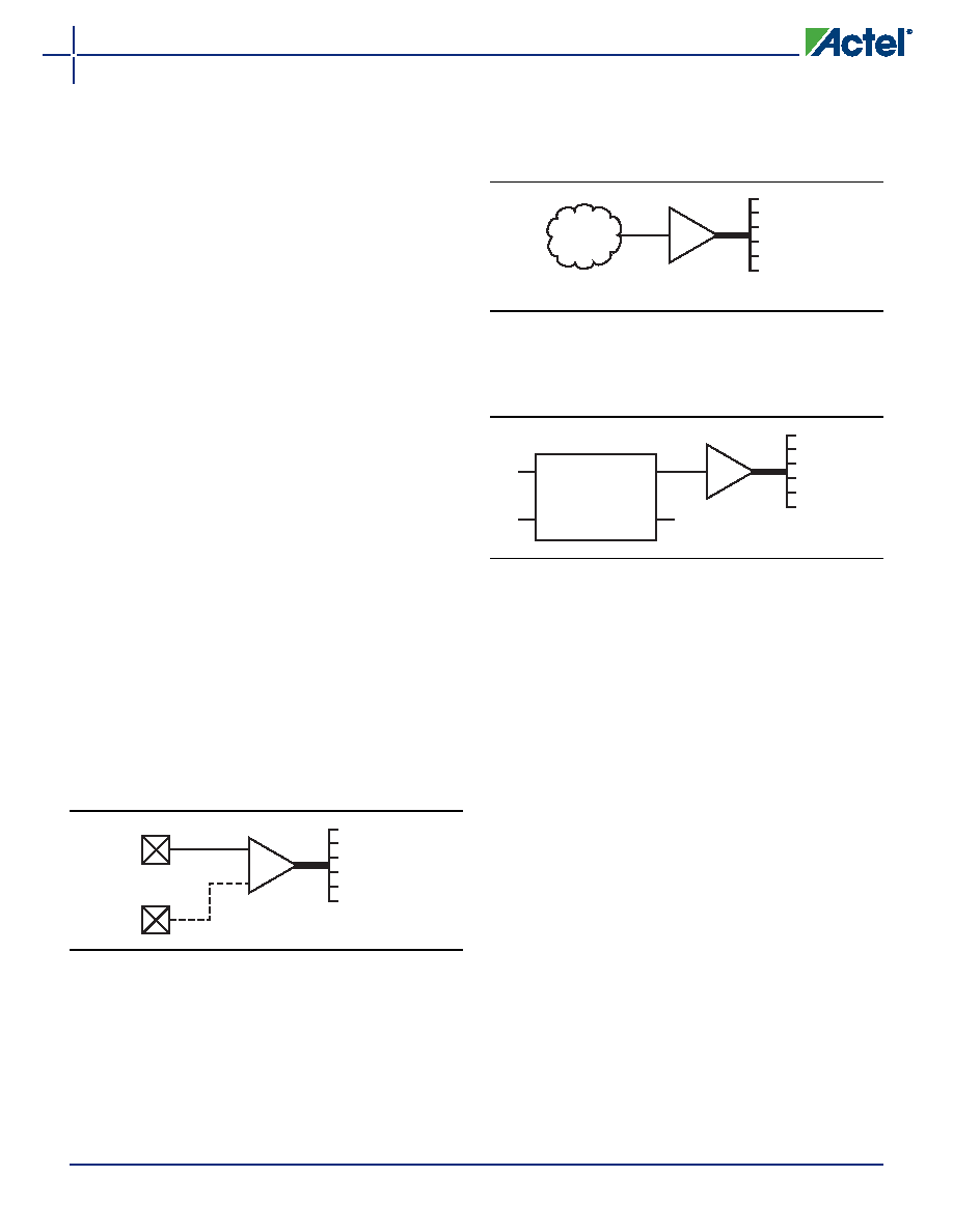
Figure 2-42 CLKBUF and HCLKBUF
P
N
CLKBUF
HCLKBUF
Clock
Network
Figure 2-43 CLKINT and HCLKINT
Figure 2-44 PLLRCLK and PLLHCLK
CLKINT
HCLKINT
Clock
Network
Logic
PLLRCLK
PLLHCLK
Clock
Network
CLK1
CLK2
FB
RefCLK
PLL
相关PDF资料 |
PDF描述 |
|---|---|
| AX125-1CS180 | FPGA, 1344 CLBS, 82000 GATES, 763 MHz, PBGA180 |
| AX125-1FG256I | FPGA, 1344 CLBS, 82000 GATES, 763 MHz, PBGA256 |
| AX125-1FG256 | FPGA, 1344 CLBS, 82000 GATES, 763 MHz, PBGA256 |
| AX125-1FG324I | FPGA, 1344 CLBS, 82000 GATES, 763 MHz, PBGA324 |
| AX125-1FG324 | FPGA, 1344 CLBS, 82000 GATES, 763 MHz, PBGA324 |
相关代理商/技术参数 |
参数描述 |
|---|---|
| AX125-1CS896 | 制造商:ACTEL 制造商全称:Actel Corporation 功能描述:Axcelerator Family FPGAs |
| AX125-1CS896B | 制造商:ACTEL 制造商全称:Actel Corporation 功能描述:Axcelerator Family FPGAs |
| AX125-1CS896I | 制造商:ACTEL 制造商全称:Actel Corporation 功能描述:Axcelerator Family FPGAs |
| AX125-1CS896M | 制造商:ACTEL 制造商全称:Actel Corporation 功能描述:Axcelerator Family FPGAs |
| AX125-1CS896PP | 制造商:ACTEL 制造商全称:Actel Corporation 功能描述:Axcelerator Family FPGAs |
发布紧急采购,3分钟左右您将得到回复。