- 您现在的位置:买卖IC网 > PDF目录295118 > AX125-1CS180I FPGA, 1344 CLBS, 82000 GATES, 763 MHz, PBGA180 PDF资料下载
参数资料
| 型号: | AX125-1CS180I |
| 元件分类: | FPGA |
| 英文描述: | FPGA, 1344 CLBS, 82000 GATES, 763 MHz, PBGA180 |
| 封装: | 0.80 MM PITCH, CSP-180 |
| 文件页数: | 218/230页 |
| 文件大小: | 6485K |
| 代理商: | AX125-1CS180I |
第1页第2页第3页第4页第5页第6页第7页第8页第9页第10页第11页第12页第13页第14页第15页第16页第17页第18页第19页第20页第21页第22页第23页第24页第25页第26页第27页第28页第29页第30页第31页第32页第33页第34页第35页第36页第37页第38页第39页第40页第41页第42页第43页第44页第45页第46页第47页第48页第49页第50页第51页第52页第53页第54页第55页第56页第57页第58页第59页第60页第61页第62页第63页第64页第65页第66页第67页第68页第69页第70页第71页第72页第73页第74页第75页第76页第77页第78页第79页第80页第81页第82页第83页第84页第85页第86页第87页第88页第89页第90页第91页第92页第93页第94页第95页第96页第97页第98页第99页第100页第101页第102页第103页第104页第105页第106页第107页第108页第109页第110页第111页第112页第113页第114页第115页第116页第117页第118页第119页第120页第121页第122页第123页第124页第125页第126页第127页第128页第129页第130页第131页第132页第133页第134页第135页第136页第137页第138页第139页第140页第141页第142页第143页第144页第145页第146页第147页第148页第149页第150页第151页第152页第153页第154页第155页第156页第157页第158页第159页第160页第161页第162页第163页第164页第165页第166页第167页第168页第169页第170页第171页第172页第173页第174页第175页第176页第177页第178页第179页第180页第181页第182页第183页第184页第185页第186页第187页第188页第189页第190页第191页第192页第193页第194页第195页第196页第197页第198页第199页第200页第201页第202页第203页第204页第205页第206页第207页第208页第209页第210页第211页第212页第213页第214页第215页第216页第217页当前第218页第219页第220页第221页第222页第223页第224页第225页第226页第227页第228页第229页第230页
Axcelerator Family FPGAs
2- 74
v2.8
Modes of Operation
There are two read modes and one write mode:
Read Nonpipelined (synchronous – one clock edge)
Read Pipelined (synchronous – two clock edges)
Write (synchronous – one clock edge)
In the standard read mode, new data is driven onto the
RD bus in the clock cycle immediately following RA and
REN valid. The read address is registered on the read-
port active-clock edge and data appears at read-data
after the RAM access time. Setting the PIPE to OFF
enables this mode.
The pipelined mode incurs an additional clock delay
from address to data, but enables operation at a much
higher frequency. The read-address is registered on the
read-port active-clock edge, and the read data is
registered and appears at RD after the second read clock
edge. Setting the PIPE to ON enables this mode.
On the write active-clock edge, the write data are
written into the SRAM at the write address when WEN is
high. The setup time of the write address, write enables,
and write data are minimal with respect to the write
clock.
Write and read transfers are described with timing
requirements beginning in "Timing Characteristics".
Timing Characteristics
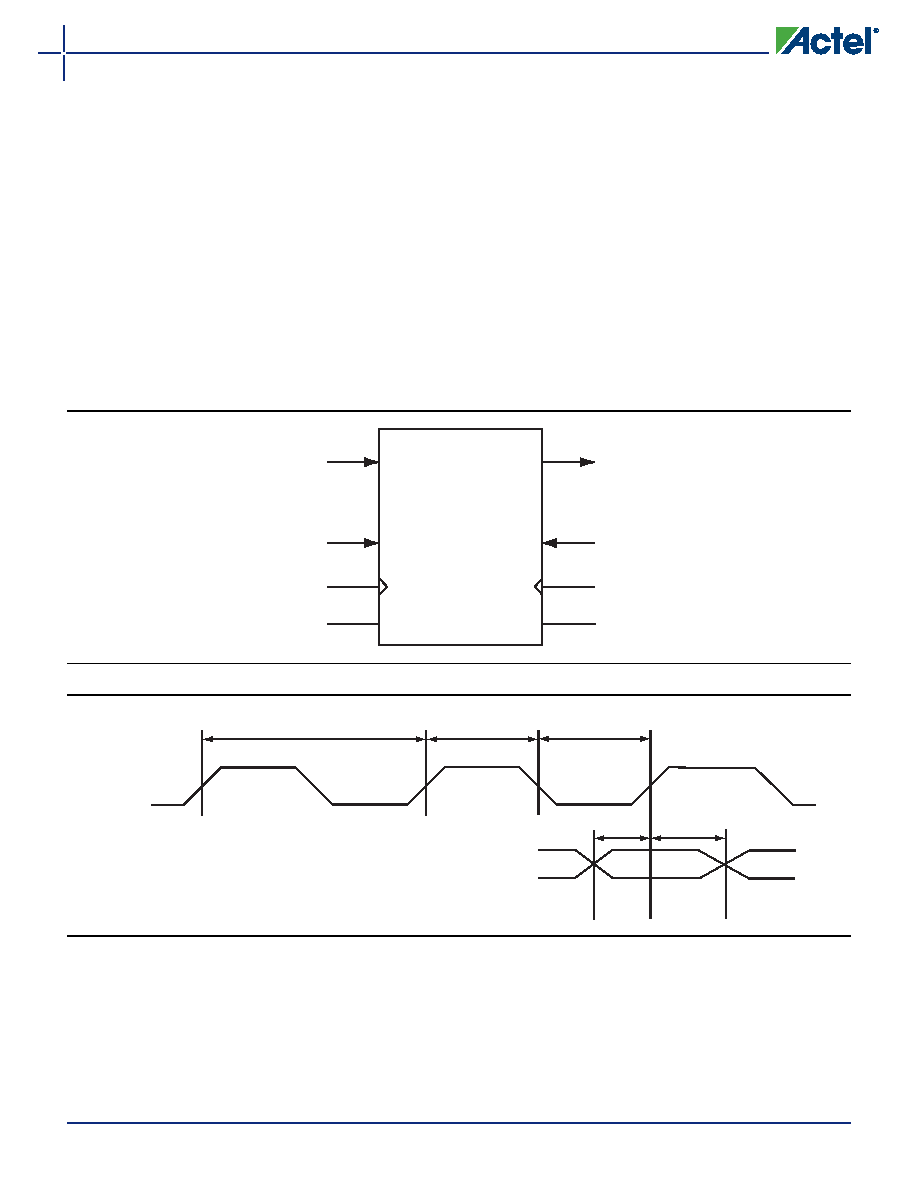
Figure 2-58 SRAM Model
Figure 2-59 RAM Write Timing Waveforms
WD
RD
RA
REN
WA
WCLK
RCLK
WEN
WCLK
tWCKP
tWxxSU
tWxxHD
tWCKH
tWCKL
WA<11:0>, WD<35:0>, WEN<4:0>
相关PDF资料 |
PDF描述 |
|---|---|
| AX125-1CS180 | FPGA, 1344 CLBS, 82000 GATES, 763 MHz, PBGA180 |
| AX125-1FG256I | FPGA, 1344 CLBS, 82000 GATES, 763 MHz, PBGA256 |
| AX125-1FG256 | FPGA, 1344 CLBS, 82000 GATES, 763 MHz, PBGA256 |
| AX125-1FG324I | FPGA, 1344 CLBS, 82000 GATES, 763 MHz, PBGA324 |
| AX125-1FG324 | FPGA, 1344 CLBS, 82000 GATES, 763 MHz, PBGA324 |
相关代理商/技术参数 |
参数描述 |
|---|---|
| AX125-1CS896 | 制造商:ACTEL 制造商全称:Actel Corporation 功能描述:Axcelerator Family FPGAs |
| AX125-1CS896B | 制造商:ACTEL 制造商全称:Actel Corporation 功能描述:Axcelerator Family FPGAs |
| AX125-1CS896I | 制造商:ACTEL 制造商全称:Actel Corporation 功能描述:Axcelerator Family FPGAs |
| AX125-1CS896M | 制造商:ACTEL 制造商全称:Actel Corporation 功能描述:Axcelerator Family FPGAs |
| AX125-1CS896PP | 制造商:ACTEL 制造商全称:Actel Corporation 功能描述:Axcelerator Family FPGAs |
发布紧急采购,3分钟左右您将得到回复。