- 您现在的位置:买卖IC网 > PDF目录295118 > AX125-1CS180I FPGA, 1344 CLBS, 82000 GATES, 763 MHz, PBGA180 PDF资料下载
参数资料
| 型号: | AX125-1CS180I |
| 元件分类: | FPGA |
| 英文描述: | FPGA, 1344 CLBS, 82000 GATES, 763 MHz, PBGA180 |
| 封装: | 0.80 MM PITCH, CSP-180 |
| 文件页数: | 24/230页 |
| 文件大小: | 6485K |
| 代理商: | AX125-1CS180I |
第1页第2页第3页第4页第5页第6页第7页第8页第9页第10页第11页第12页第13页第14页第15页第16页第17页第18页第19页第20页第21页第22页第23页当前第24页第25页第26页第27页第28页第29页第30页第31页第32页第33页第34页第35页第36页第37页第38页第39页第40页第41页第42页第43页第44页第45页第46页第47页第48页第49页第50页第51页第52页第53页第54页第55页第56页第57页第58页第59页第60页第61页第62页第63页第64页第65页第66页第67页第68页第69页第70页第71页第72页第73页第74页第75页第76页第77页第78页第79页第80页第81页第82页第83页第84页第85页第86页第87页第88页第89页第90页第91页第92页第93页第94页第95页第96页第97页第98页第99页第100页第101页第102页第103页第104页第105页第106页第107页第108页第109页第110页第111页第112页第113页第114页第115页第116页第117页第118页第119页第120页第121页第122页第123页第124页第125页第126页第127页第128页第129页第130页第131页第132页第133页第134页第135页第136页第137页第138页第139页第140页第141页第142页第143页第144页第145页第146页第147页第148页第149页第150页第151页第152页第153页第154页第155页第156页第157页第158页第159页第160页第161页第162页第163页第164页第165页第166页第167页第168页第169页第170页第171页第172页第173页第174页第175页第176页第177页第178页第179页第180页第181页第182页第183页第184页第185页第186页第187页第188页第189页第190页第191页第192页第193页第194页第195页第196页第197页第198页第199页第200页第201页第202页第203页第204页第205页第206页第207页第208页第209页第210页第211页第212页第213页第214页第215页第216页第217页第218页第219页第220页第221页第222页第223页第224页第225页第226页第227页第228页第229页第230页
Axcelerator Family FPGAs
1- 6
v2.8
operating with input frequencies ranging from 14 MHz
to 200 MHz and can generate output frequencies
between 20 MHz and 1 GHz. The clock can be either
divided or multiplied by factors ranging from 1 to 64.
Additionally, multiply and divide settings can be used in
any combination as long as the resulting clock frequency
is between 20 MHz and 1 GHz. Adjacent PLLs can be
cascaded to create complex frequency combinations.
The PLL can be used to introduce either a positive or a
negative clock delay of up to 3.75 ns in 250 ps
increments. The reference clock required to drive the PLL
can be derived from three sources: external input pad
(either single-ended or differential), internal logic, or the
output of an adjacent PLL.
Low Power (LP) Mode
The AX architecture was created for high-performance
designs but also includes a low power mode (activated via
the LP pin). When the low power mode is activated, I/O
banks can be disabled (inputs disabled, outputs tristated),
and PLLs can be placed in a power-down mode. All
internal register states are maintained in this mode.
Furthermore, individual I/O banks can be configured to
opt out of the LP mode, thereby giving the designer access
to critical signals while the rest of the chip is in low power
mode.
The power can be further reduced by providing an
external voltage source (VPUMP) to the device to bypass
the internal charge pump (See "Low Power Mode" on
page 2-89 for more information).
Design Environment
The Axcelerator family of FPGAs is fully supported by both
Actel's Libero Integrated Design Environment and
Designer FPGA Development software. Actel Libero IDE is
an integrated design manager that seamlessly integrates
design tools while guiding the user through the design
flow, managing all design and log files, and passing
necessary design data among tools. Additionally, Libero
IDE allows users to integrate both schematic and HDL
synthesis into a single flow and verify the entire design in
a single environment (see the Libero IDE Flow diagram
located on Actel’s website). Libero IDE includes Synplify
Actel Edition (AE) from Synplicity, ViewDraw AE from
Mentor Graphics, ModelSim HDL Simulator from
Mentor
Graphics,
WaveFormer
Lite
AE
from
SynaptiCAD, and Designer software from Actel.
Actel's Designer software is a place-and-route tool and
provides a comprehensive suite of backend support tools
for FPGA development. The Designer software includes
the following:
Timer – a world-class integrated static timing analyzer
and constraints editor which support timing-driven
place-and-route
NetlistViewer – a design netlist schematic viewer
ChipPlanner – a graphical floorplanner viewer and editor
SmartPower – allows the designer to quickly estimate
the power consumption of a design
PinEditor – a graphical application for editing pin
assignments and I/O attributes
I/O Attribute Editor – displays all assigned and
unassigned I/O macros and their attributes in a
spreadsheet format
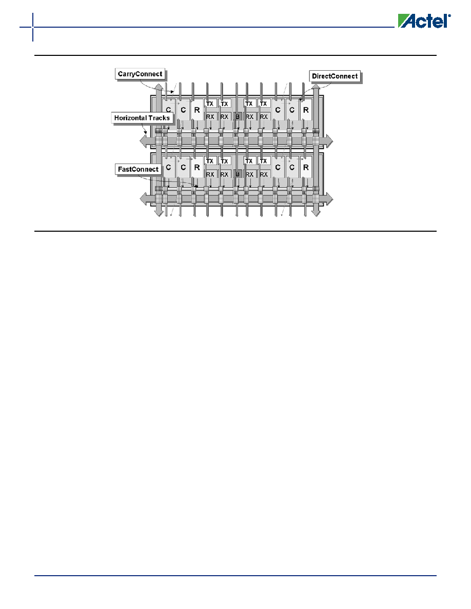
Figure 1-8 AX Routing Structures
相关PDF资料 |
PDF描述 |
|---|---|
| AX125-1CS180 | FPGA, 1344 CLBS, 82000 GATES, 763 MHz, PBGA180 |
| AX125-1FG256I | FPGA, 1344 CLBS, 82000 GATES, 763 MHz, PBGA256 |
| AX125-1FG256 | FPGA, 1344 CLBS, 82000 GATES, 763 MHz, PBGA256 |
| AX125-1FG324I | FPGA, 1344 CLBS, 82000 GATES, 763 MHz, PBGA324 |
| AX125-1FG324 | FPGA, 1344 CLBS, 82000 GATES, 763 MHz, PBGA324 |
相关代理商/技术参数 |
参数描述 |
|---|---|
| AX125-1CS896 | 制造商:ACTEL 制造商全称:Actel Corporation 功能描述:Axcelerator Family FPGAs |
| AX125-1CS896B | 制造商:ACTEL 制造商全称:Actel Corporation 功能描述:Axcelerator Family FPGAs |
| AX125-1CS896I | 制造商:ACTEL 制造商全称:Actel Corporation 功能描述:Axcelerator Family FPGAs |
| AX125-1CS896M | 制造商:ACTEL 制造商全称:Actel Corporation 功能描述:Axcelerator Family FPGAs |
| AX125-1CS896PP | 制造商:ACTEL 制造商全称:Actel Corporation 功能描述:Axcelerator Family FPGAs |
发布紧急采购,3分钟左右您将得到回复。