- 您现在的位置:买卖IC网 > PDF目录17092 > C8051F005-TB (Silicon Laboratories Inc)BOARD PROTOTYPING W/C8051F005 PDF资料下载
参数资料
| 型号: | C8051F005-TB |
| 厂商: | Silicon Laboratories Inc |
| 文件页数: | 107/171页 |
| 文件大小: | 0K |
| 描述: | BOARD PROTOTYPING W/C8051F005 |
| 标准包装: | 1 |
| 类型: | MCU |
| 适用于相关产品: | C8051F005 |
| 所含物品: | 板 |
第1页第2页第3页第4页第5页第6页第7页第8页第9页第10页第11页第12页第13页第14页第15页第16页第17页第18页第19页第20页第21页第22页第23页第24页第25页第26页第27页第28页第29页第30页第31页第32页第33页第34页第35页第36页第37页第38页第39页第40页第41页第42页第43页第44页第45页第46页第47页第48页第49页第50页第51页第52页第53页第54页第55页第56页第57页第58页第59页第60页第61页第62页第63页第64页第65页第66页第67页第68页第69页第70页第71页第72页第73页第74页第75页第76页第77页第78页第79页第80页第81页第82页第83页第84页第85页第86页第87页第88页第89页第90页第91页第92页第93页第94页第95页第96页第97页第98页第99页第100页第101页第102页第103页第104页第105页第106页当前第107页第108页第109页第110页第111页第112页第113页第114页第115页第116页第117页第118页第119页第120页第121页第122页第123页第124页第125页第126页第127页第128页第129页第130页第131页第132页第133页第134页第135页第136页第137页第138页第139页第140页第141页第142页第143页第144页第145页第146页第147页第148页第149页第150页第151页第152页第153页第154页第155页第156页第157页第158页第159页第160页第161页第162页第163页第164页第165页第166页第167页第168页第169页第170页第171页
C8051F000/1/2/5/6/7
C8051F010/1/2/5/6/7
6.
ADC (10-Bit, C8051F010/1/2/5/6/7 Only)
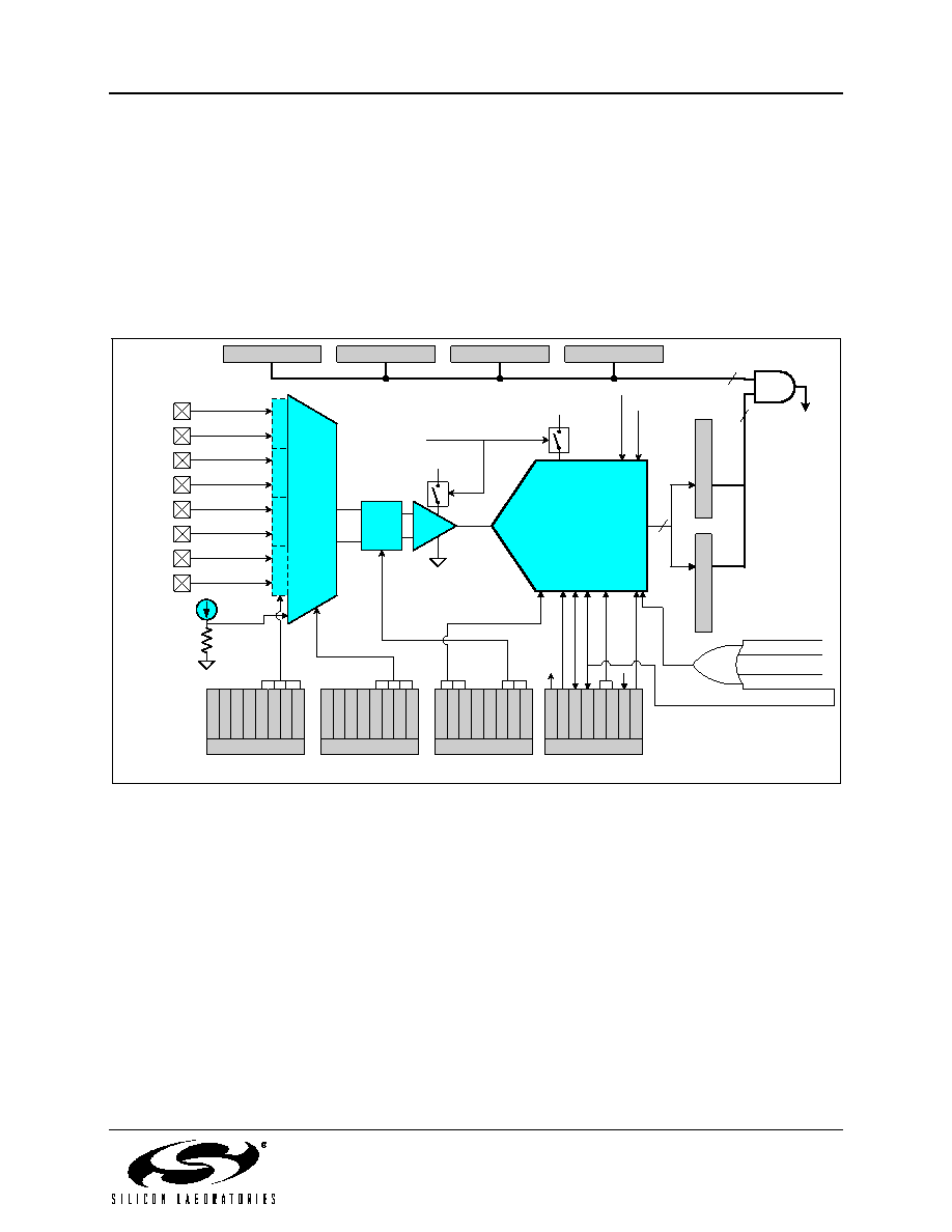
The ADC subsystem for the C8051F010/1/2/5/6/7 consists of a 9-channel, configurable analog multiplexer
(AMUX), a programmable gain amplifier (PGA), and a 100ksps, 10-bit successive-approximation-register ADC
with integrated track-and-hold and programmable window detector (see block diagram in Figure 6.1). The AMUX,
PGA, Data Conversion Modes, and Window Detector are all configurable under software control via the Special
Function Register’s shown in Figure 6.1. The ADC subsystem (ADC, track-and-hold and PGA) is enabled only
when the ADCEN bit in the ADC Control register (ADC0CN, Figure 6.7) is set to 1. The ADC subsystem is in low
power shutdown when this bit is 0. The Bias Enable bit (BIASE) in the REF0CN register (see Figure 9.2) must be
set to 1 in order to supply bias to the ADC.
Figure 6.1. 10-Bit ADC Functional Block Diagram
10-Bit
SAR
ADC
REF
+
-
AV+
TEMP
SENSOR
10
+
-
+
-
+
-
9-to-1
AMUX
(SE or
DIFF)
AV+
COMB
LOGIC
20
10
ADWINT
ADCEN
SYSCLK
+
-
X
AIN0
AIN1
AIN2
AIN3
AIN4
AIN5
AIN6
AIN7
TMR3 OV
T2 OV
CNVSTR
ADBUSY(w)
Conversion
Start
AGND
AMX0CF
AIN01IC
AIN23IC
AIN45IC
AIN67IC
AMX0SL
AMXAD0
AMXAD1
AMXAD2
AMXAD3
ADC0CF
AMPGN0
AMPGN1
AMPGN2
ADCSC0
ADCSC1
ADCSC2
ADC0CN
ADLJST
ADWINT
ADSTM0
ADSTM1
ADBUSY
ADCINT
ADCTM
ADCEN
ADC0L
ADC0H
ADC0LTL
ADC0LTH
ADC0GTL
ADC0GTH
6.1.
Analog Multiplexer and PGA
Eight of the AMUX channels are available for external measurements while the ninth channel is internally
connected to an on-board temperature sensor (temperature transfer function is shown in Figure 6.3). Note that the
PGA gain is applied to the temperature sensor reading. AMUX input pairs can be programmed to operate in either
the differential or single-ended mode. This allows the user to select the best measurement technique for each input
channel, and even accommodates mode changes “on-the-fly”. The AMUX defaults to all single-ended inputs upon
reset. There are two registers associated with the AMUX: the Channel Selection register AMX0SL (Figure 6.5),
and the Configuration register AMX0CF (Figure 6.4). The table in Figure 6.5 shows AMUX functionality by
channel for each possible configuration. The PGA amplifies the AMUX output signal by an amount determined by
the AMPGN2-0 bits in the ADC Configuration register, ADC0CF (Figure 6.6).
The PGA can be software-
programmed for gains of 0.5, 1, 2, 4, 8 or 16. It defaults to unity gain on reset.
Rev. 1.7
40
相关PDF资料 |
PDF描述 |
|---|---|
| SK101M250ST | CAP ALUM 100UF 250V 20% RADIAL |
| SLPX472M063E3P3 | CAP ALUM 4700UF 63V 20% SNAP |
| SDR-R | SCOTCH CODE REFILL R |
| C8051F206-TB | BOARD PROTOTYPING W/C8051F206 |
| 0210490992 | CABLE JUMPER 1.25MM .102M 29POS |
相关代理商/技术参数 |
参数描述 |
|---|---|
| C8051F005-TB-K | 功能描述:BOARD PROTOTYPING W/C8051F005 制造商:silicon labs 系列:- 零件状态:在售 板类型:评估平台 类型:MCU 8-位 核心处理器:8051 操作系统:- 平台:- 配套使用产品/相关产品:C8051F0xx 安装类型:固定 内容:板 标准包装:1 |
| C8051F006 | 功能描述:8位微控制器 -MCU 32KB 12ADC RoHS:否 制造商:Silicon Labs 核心:8051 处理器系列:C8051F39x 数据总线宽度:8 bit 最大时钟频率:50 MHz 程序存储器大小:16 KB 数据 RAM 大小:1 KB 片上 ADC:Yes 工作电源电压:1.8 V to 3.6 V 工作温度范围:- 40 C to + 105 C 封装 / 箱体:QFN-20 安装风格:SMD/SMT |
| C8051F006-GQ | 功能描述:8位微控制器 -MCU 32KB 12ADC RoHS:否 制造商:Silicon Labs 核心:8051 处理器系列:C8051F39x 数据总线宽度:8 bit 最大时钟频率:50 MHz 程序存储器大小:16 KB 数据 RAM 大小:1 KB 片上 ADC:Yes 工作电源电压:1.8 V to 3.6 V 工作温度范围:- 40 C to + 105 C 封装 / 箱体:QFN-20 安装风格:SMD/SMT |
| C8051F006-GQR | 功能描述:8位微控制器 -MCU 32KB 12ADC 48Pin MCU Tape and Reel RoHS:否 制造商:Silicon Labs 核心:8051 处理器系列:C8051F39x 数据总线宽度:8 bit 最大时钟频率:50 MHz 程序存储器大小:16 KB 数据 RAM 大小:1 KB 片上 ADC:Yes 工作电源电压:1.8 V to 3.6 V 工作温度范围:- 40 C to + 105 C 封装 / 箱体:QFN-20 安装风格:SMD/SMT |
| C8051F006R | 功能描述:8位微控制器 -MCU C +-12Bit 48Pin RoHS:否 制造商:Silicon Labs 核心:8051 处理器系列:C8051F39x 数据总线宽度:8 bit 最大时钟频率:50 MHz 程序存储器大小:16 KB 数据 RAM 大小:1 KB 片上 ADC:Yes 工作电源电压:1.8 V to 3.6 V 工作温度范围:- 40 C to + 105 C 封装 / 箱体:QFN-20 安装风格:SMD/SMT |
发布紧急采购,3分钟左右您将得到回复。