- 您现在的位置:买卖IC网 > PDF目录17092 > C8051F005-TB (Silicon Laboratories Inc)BOARD PROTOTYPING W/C8051F005 PDF资料下载
参数资料
| 型号: | C8051F005-TB |
| 厂商: | Silicon Laboratories Inc |
| 文件页数: | 82/171页 |
| 文件大小: | 0K |
| 描述: | BOARD PROTOTYPING W/C8051F005 |
| 标准包装: | 1 |
| 类型: | MCU |
| 适用于相关产品: | C8051F005 |
| 所含物品: | 板 |
第1页第2页第3页第4页第5页第6页第7页第8页第9页第10页第11页第12页第13页第14页第15页第16页第17页第18页第19页第20页第21页第22页第23页第24页第25页第26页第27页第28页第29页第30页第31页第32页第33页第34页第35页第36页第37页第38页第39页第40页第41页第42页第43页第44页第45页第46页第47页第48页第49页第50页第51页第52页第53页第54页第55页第56页第57页第58页第59页第60页第61页第62页第63页第64页第65页第66页第67页第68页第69页第70页第71页第72页第73页第74页第75页第76页第77页第78页第79页第80页第81页当前第82页第83页第84页第85页第86页第87页第88页第89页第90页第91页第92页第93页第94页第95页第96页第97页第98页第99页第100页第101页第102页第103页第104页第105页第106页第107页第108页第109页第110页第111页第112页第113页第114页第115页第116页第117页第118页第119页第120页第121页第122页第123页第124页第125页第126页第127页第128页第129页第130页第131页第132页第133页第134页第135页第136页第137页第138页第139页第140页第141页第142页第143页第144页第145页第146页第147页第148页第149页第150页第151页第152页第153页第154页第155页第156页第157页第158页第159页第160页第161页第162页第163页第164页第165页第166页第167页第168页第169页第170页第171页
C8051F000/1/2/5/6/7
C8051F010/1/2/5/6/7
1.7.
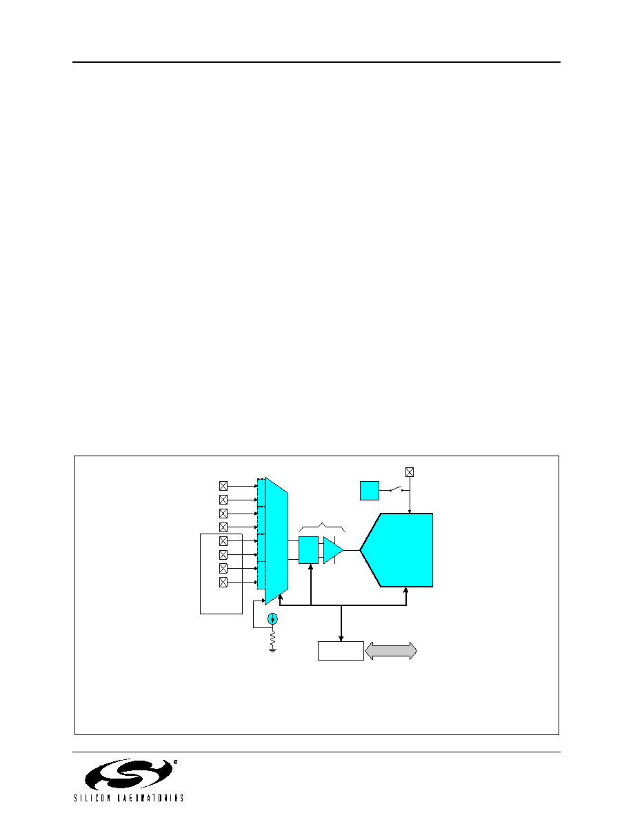
Analog to Digital Converter
The C8051F000/1/2/5/6/7 has an on-chip 12-bit SAR ADC with a 9-channel input multiplexer and programmable
gain amplifier. With a maximum throughput of 100ksps, the ADC offers true 12-bit accuracy with an INL of
1LSB. The ADC in the C8051F010/1/2/5/6/7 is similar, but with 10-bit resolution. Each ADC has a maximum
throughput of 100ksps. Each ADC has an INL of
1LSB, offering true 12-bit accuracy with the C8051F00x, and
true 10-bit accuracy with the C8051F01x. There is also an on-board 15ppm voltage reference, or an external
reference may be used via the VREF pin.
The ADC is under full control of the CIP-51 microcontroller via the Special Function Registers. One input channel
is tied to an internal temperature sensor, while the other eight channels are available externally. Each pair of the
eight external input channels can be configured as either two single-ended inputs or a single differential input. The
system controller can also put the ADC into shutdown to save power.
A programmable gain amplifier follows the analog multiplexer. The gain can be set in software from 0.5 to 16 in
powers of 2. The gain stage can be especially useful when different ADC input channels have widely varied input
voltage signals, or when it is necessary to “zoom in” on a signal with a large DC offset (in differential mode, a DAC
could be used to provide the DC offset).
Conversions can be started in four ways; a software command, an overflow on Timer 2, an overflow on Timer 3, or
an external signal input. This flexibility allows the start of conversion to be triggered by software events, external
HW signals, or convert continuously. A completed conversion causes an interrupt, or a status bit can be polled in
software to determine the end of conversion. The resulting 10 or 12-bit data word is latched into two SFRs upon
completion of a conversion. The data can be right or left justified in these registers under software control.
Compare registers for the ADC data can be configured to interrupt the controller when ADC data is within a
specified window. The ADC can monitor a key voltage continuously in background mode, but not interrupt the
controller unless the converted data is within the specified window.
Figure 1.10. ADC Diagram
100ksps
SAR
ADC
+
-
Control & Data
SFR's
SFR Bus
+
-
+
-
+
-
9-to-1
AMUX
(SE or
DIFF)
+
-
X
AIN0
AIN1
AIN2
AIN3
AIN4
AIN5
AIN6
AIN7
TEMP
SENSOR
Programmable
Gain Amp
VREF
REF
(not bonded out on
F002, F007, F012,
and F017
Rev. 1.7
18
相关PDF资料 |
PDF描述 |
|---|---|
| SK101M250ST | CAP ALUM 100UF 250V 20% RADIAL |
| SLPX472M063E3P3 | CAP ALUM 4700UF 63V 20% SNAP |
| SDR-R | SCOTCH CODE REFILL R |
| C8051F206-TB | BOARD PROTOTYPING W/C8051F206 |
| 0210490992 | CABLE JUMPER 1.25MM .102M 29POS |
相关代理商/技术参数 |
参数描述 |
|---|---|
| C8051F005-TB-K | 功能描述:BOARD PROTOTYPING W/C8051F005 制造商:silicon labs 系列:- 零件状态:在售 板类型:评估平台 类型:MCU 8-位 核心处理器:8051 操作系统:- 平台:- 配套使用产品/相关产品:C8051F0xx 安装类型:固定 内容:板 标准包装:1 |
| C8051F006 | 功能描述:8位微控制器 -MCU 32KB 12ADC RoHS:否 制造商:Silicon Labs 核心:8051 处理器系列:C8051F39x 数据总线宽度:8 bit 最大时钟频率:50 MHz 程序存储器大小:16 KB 数据 RAM 大小:1 KB 片上 ADC:Yes 工作电源电压:1.8 V to 3.6 V 工作温度范围:- 40 C to + 105 C 封装 / 箱体:QFN-20 安装风格:SMD/SMT |
| C8051F006-GQ | 功能描述:8位微控制器 -MCU 32KB 12ADC RoHS:否 制造商:Silicon Labs 核心:8051 处理器系列:C8051F39x 数据总线宽度:8 bit 最大时钟频率:50 MHz 程序存储器大小:16 KB 数据 RAM 大小:1 KB 片上 ADC:Yes 工作电源电压:1.8 V to 3.6 V 工作温度范围:- 40 C to + 105 C 封装 / 箱体:QFN-20 安装风格:SMD/SMT |
| C8051F006-GQR | 功能描述:8位微控制器 -MCU 32KB 12ADC 48Pin MCU Tape and Reel RoHS:否 制造商:Silicon Labs 核心:8051 处理器系列:C8051F39x 数据总线宽度:8 bit 最大时钟频率:50 MHz 程序存储器大小:16 KB 数据 RAM 大小:1 KB 片上 ADC:Yes 工作电源电压:1.8 V to 3.6 V 工作温度范围:- 40 C to + 105 C 封装 / 箱体:QFN-20 安装风格:SMD/SMT |
| C8051F006R | 功能描述:8位微控制器 -MCU C +-12Bit 48Pin RoHS:否 制造商:Silicon Labs 核心:8051 处理器系列:C8051F39x 数据总线宽度:8 bit 最大时钟频率:50 MHz 程序存储器大小:16 KB 数据 RAM 大小:1 KB 片上 ADC:Yes 工作电源电压:1.8 V to 3.6 V 工作温度范围:- 40 C to + 105 C 封装 / 箱体:QFN-20 安装风格:SMD/SMT |
发布紧急采购,3分钟左右您将得到回复。