- 您现在的位置:买卖IC网 > PDF目录17092 > C8051F005-TB (Silicon Laboratories Inc)BOARD PROTOTYPING W/C8051F005 PDF资料下载
参数资料
| 型号: | C8051F005-TB |
| 厂商: | Silicon Laboratories Inc |
| 文件页数: | 119/171页 |
| 文件大小: | 0K |
| 描述: | BOARD PROTOTYPING W/C8051F005 |
| 标准包装: | 1 |
| 类型: | MCU |
| 适用于相关产品: | C8051F005 |
| 所含物品: | 板 |
第1页第2页第3页第4页第5页第6页第7页第8页第9页第10页第11页第12页第13页第14页第15页第16页第17页第18页第19页第20页第21页第22页第23页第24页第25页第26页第27页第28页第29页第30页第31页第32页第33页第34页第35页第36页第37页第38页第39页第40页第41页第42页第43页第44页第45页第46页第47页第48页第49页第50页第51页第52页第53页第54页第55页第56页第57页第58页第59页第60页第61页第62页第63页第64页第65页第66页第67页第68页第69页第70页第71页第72页第73页第74页第75页第76页第77页第78页第79页第80页第81页第82页第83页第84页第85页第86页第87页第88页第89页第90页第91页第92页第93页第94页第95页第96页第97页第98页第99页第100页第101页第102页第103页第104页第105页第106页第107页第108页第109页第110页第111页第112页第113页第114页第115页第116页第117页第118页当前第119页第120页第121页第122页第123页第124页第125页第126页第127页第128页第129页第130页第131页第132页第133页第134页第135页第136页第137页第138页第139页第140页第141页第142页第143页第144页第145页第146页第147页第148页第149页第150页第151页第152页第153页第154页第155页第156页第157页第158页第159页第160页第161页第162页第163页第164页第165页第166页第167页第168页第169页第170页第171页
C8051F000/1/2/5/6/7
C8051F010/1/2/5/6/7
7.
DACs, 12 BIT VOLTAGE MODE
The C8051F000 MCU family has two 12-bit voltage-mode Digital to Analog Converters. Each DAC has an output
swing of 0V to VREF-1LSB for a corresponding input code range of 0x000 to 0xFFF. Using DAC0 as an example,
the 12-bit data word is written to the low byte (DAC0L) and high byte (DAC0H) data registers. Data is latched into
DAC0 after a write to the corresponding DAC0H register, so the write sequence should be DAC0L followed by
DAC0H if the full 12-bit resolution is required. The DAC can be used in 8-bit mode by initializing DAC0L to the
desired value (typically 0x00), and writing data to only DAC0H with the data shifted to the left. DAC0 Control
Register (DAC0CN) provides a means to enable/disable DAC0 and to modify its input data formatting.
The DAC0 enable/disable function is controlled by the DAC0EN bit (DAC0CN.7). Writing a 1 to DAC0EN
enables DAC0 while writing a 0 to DAC0EN disables DAC0. While disabled, the output of DAC0 is maintained in
a high-impedance state, and the DAC0 supply current falls to 1
A or less. Also, the Bias Enable bit (BIASE) in the
REF0CN register (see Figure 9.2) must be set to 1 in order to supply bias to DAC0. The voltage reference for
DAC0 must also be set properly (see Section 9).
In some instances, input data should be shifted prior to a DAC0 write operation to properly justify data within the
DAC input registers. This action would typically require one or more load and shift operations, adding software
overhead and slowing DAC throughput. To alleviate this problem, the data-formatting feature provides a means for
the user to program the orientation of the DAC0 data word within data registers DAC0H and DAC0L. The three
DAC0DF bits (DAC0CN.[2:0]) allow the user to specify one of five data word orientations as shown in the
DAC0CN register definition.
DAC1 is functionally the same as DAC0 described above. The electrical specifications for both DAC0 and DAC1
are given in Table 7.1.
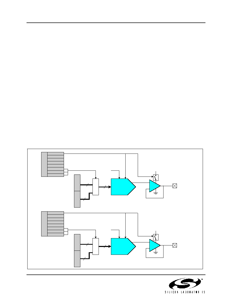
Figure 7.1. DAC Functional Block Diagram
DAC0
+
-
AV+
12
AGND
8
REF
DAC0
DAC0CN
DAC0EN
DAC0DF2
DAC0DF1
DAC0DF0
DAC0H
DAC0L
Dig.
MUX
DAC1
+
-
AV+
12
AGND
8
REF
DAC1
DAC1CN
DAC1EN
DAC1DF2
DAC1DF1
DAC1DF0
DAC1H
DAC1L
Dig.
MUX
51
Rev. 1.7
相关PDF资料 |
PDF描述 |
|---|---|
| SK101M250ST | CAP ALUM 100UF 250V 20% RADIAL |
| SLPX472M063E3P3 | CAP ALUM 4700UF 63V 20% SNAP |
| SDR-R | SCOTCH CODE REFILL R |
| C8051F206-TB | BOARD PROTOTYPING W/C8051F206 |
| 0210490992 | CABLE JUMPER 1.25MM .102M 29POS |
相关代理商/技术参数 |
参数描述 |
|---|---|
| C8051F005-TB-K | 功能描述:BOARD PROTOTYPING W/C8051F005 制造商:silicon labs 系列:- 零件状态:在售 板类型:评估平台 类型:MCU 8-位 核心处理器:8051 操作系统:- 平台:- 配套使用产品/相关产品:C8051F0xx 安装类型:固定 内容:板 标准包装:1 |
| C8051F006 | 功能描述:8位微控制器 -MCU 32KB 12ADC RoHS:否 制造商:Silicon Labs 核心:8051 处理器系列:C8051F39x 数据总线宽度:8 bit 最大时钟频率:50 MHz 程序存储器大小:16 KB 数据 RAM 大小:1 KB 片上 ADC:Yes 工作电源电压:1.8 V to 3.6 V 工作温度范围:- 40 C to + 105 C 封装 / 箱体:QFN-20 安装风格:SMD/SMT |
| C8051F006-GQ | 功能描述:8位微控制器 -MCU 32KB 12ADC RoHS:否 制造商:Silicon Labs 核心:8051 处理器系列:C8051F39x 数据总线宽度:8 bit 最大时钟频率:50 MHz 程序存储器大小:16 KB 数据 RAM 大小:1 KB 片上 ADC:Yes 工作电源电压:1.8 V to 3.6 V 工作温度范围:- 40 C to + 105 C 封装 / 箱体:QFN-20 安装风格:SMD/SMT |
| C8051F006-GQR | 功能描述:8位微控制器 -MCU 32KB 12ADC 48Pin MCU Tape and Reel RoHS:否 制造商:Silicon Labs 核心:8051 处理器系列:C8051F39x 数据总线宽度:8 bit 最大时钟频率:50 MHz 程序存储器大小:16 KB 数据 RAM 大小:1 KB 片上 ADC:Yes 工作电源电压:1.8 V to 3.6 V 工作温度范围:- 40 C to + 105 C 封装 / 箱体:QFN-20 安装风格:SMD/SMT |
| C8051F006R | 功能描述:8位微控制器 -MCU C +-12Bit 48Pin RoHS:否 制造商:Silicon Labs 核心:8051 处理器系列:C8051F39x 数据总线宽度:8 bit 最大时钟频率:50 MHz 程序存储器大小:16 KB 数据 RAM 大小:1 KB 片上 ADC:Yes 工作电源电压:1.8 V to 3.6 V 工作温度范围:- 40 C to + 105 C 封装 / 箱体:QFN-20 安装风格:SMD/SMT |
发布紧急采购,3分钟左右您将得到回复。