参数资料
| 型号: | C8051F018 |
| 厂商: | Silicon Laboratories Inc |
| 文件页数: | 153/154页 |
| 文件大小: | 0K |
| 描述: | IC 8051 MCU 16K FLASH 64TQFP |
| 标准包装: | 160 |
| 系列: | C8051F018 |
| 核心处理器: | 8051 |
| 芯体尺寸: | 8-位 |
| 速度: | 25MHz |
| 连通性: | SMBus(2 线/I²C),SPI,UART/USART |
| 外围设备: | 欠压检测/复位,POR,PWM,温度传感器,WDT |
| 输入/输出数: | 32 |
| 程序存储器容量: | 16KB(16K x 8) |
| 程序存储器类型: | 闪存 |
| RAM 容量: | 1.25K x 8 |
| 电压 - 电源 (Vcc/Vdd): | 2.8 V ~ 3.6 V |
| 数据转换器: | A/D 8x10b |
| 振荡器型: | 内部 |
| 工作温度: | -40°C ~ 85°C |
| 封装/外壳: | 64-TQFP |
| 包装: | 托盘 |
第1页第2页第3页第4页第5页第6页第7页第8页第9页第10页第11页第12页第13页第14页第15页第16页第17页第18页第19页第20页第21页第22页第23页第24页第25页第26页第27页第28页第29页第30页第31页第32页第33页第34页第35页第36页第37页第38页第39页第40页第41页第42页第43页第44页第45页第46页第47页第48页第49页第50页第51页第52页第53页第54页第55页第56页第57页第58页第59页第60页第61页第62页第63页第64页第65页第66页第67页第68页第69页第70页第71页第72页第73页第74页第75页第76页第77页第78页第79页第80页第81页第82页第83页第84页第85页第86页第87页第88页第89页第90页第91页第92页第93页第94页第95页第96页第97页第98页第99页第100页第101页第102页第103页第104页第105页第106页第107页第108页第109页第110页第111页第112页第113页第114页第115页第116页第117页第118页第119页第120页第121页第122页第123页第124页第125页第126页第127页第128页第129页第130页第131页第132页第133页第134页第135页第136页第137页第138页第139页第140页第141页第142页第143页第144页第145页第146页第147页第148页第149页第150页第151页第152页当前第153页第154页
C8051F018
C8051F019
14.2.
Operation
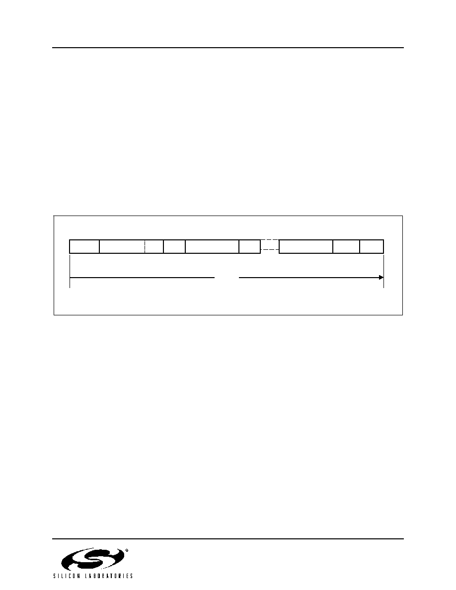
A typical SMBus transaction consists of a START condition, followed by an address byte, one or more bytes of
data, and a STOP condition. The address byte and each of the data bytes are followed by an ACKNOWLEDGE bit
from the receiver. The address byte consists of a 7-bit address plus a direction bit. The direction bit (R/W)
occupies the least-significant bit position of the address. The direction bit is set to logic 1 to indicate a “READ”
operation and cleared to logic 0 to indicate a “WRITE” operation.
A general call address (0x00 +R/W) is
recognized by all slave devices allowing a master to address multiple slave devices simultaneously.
All transactions are initiated by the master, with one or more addressed slave devices as the target.
The master
generates the START condition and then transmits the address and direction bit. If the transaction is a WRITE
operation from the master to the slave, the master transmits the data a byte at a time waiting for an
ACKNOWLEDGE from the slave at the end of each byte. If it is a READ operation, the slave transmits the data
waiting for an ACKNOWLEDGE from the master at the end of each byte. At the end of the data transfer, the
master generates a STOP condition to terminate the transaction and free the bus. Figure 14.3 illustrates a typical
SMBus transaction.
Figure 14.3. SMBus Transaction
The SMBus interface may be configured to operate as either a master or a slave. At any particular time, it will be
operating in one of the following four modes:
14.2.1. Master Transmitter Mode
Serial data is transmitted on SDA while the serial clock is output on SCL. The first byte transmitted contains the
address of the target slave device and the data direction bit. In this case the data direction bit (R/W) will be logic 0
to indicate a “WRITE” operation. The master then transmits one or more bytes of serial data. After each byte is
transmitted, an acknowledge bit is generated by the slave. To indicate the beginning and the end of the serial
transfer, the master device outputs START and STOP conditions.
14.2.2. Master Receiver Mode
Serial data is received on SDA while the serial clock is output on SCL. The first byte is transmitted by the master
and contains the address of the target slave and the data direction bit. In this case the data direction bit (R/W) will
be logic 1 to indicate a “READ” operation.
Serial data is then received from the slave on SDA while the master
outputs the serial clock. The slave transmits one or more bytes of serial data. After each byte is received, an
acknowledge bit is transmitted by the master. The master outputs START and STOP conditions to indicate the
beginning and end of the serial transfer.
14.2.3. Slave Transmitter Mode
Serial data is transmitted on SDA while the serial clock is received on SCL. First, a byte is received that contains an
address and data direction bit. In this case the data direction bit (R/W) will be logic 1 to indicate a “READ”
operation. If the received address matches the slave’s assigned address (or a general call address is received) one or
more bytes of serial data are transmitted to the master.
After each byte is received, an acknowledge bit is
transmitted by the master. The master outputs START and STOP conditions to indicate the beginning and end of
the serial transfer.
START
SLAVE ADDR
R/W
ACK
DATA
ACK
DATA
NACK
STOP
Time
Rev. 1.2
98
相关PDF资料 |
PDF描述 |
|---|---|
| DSPIC33EP256MU814-I/PL | IC DSC 16BIT 256KB 144LQFP |
| 106457-7 | Z-PACK/A SPACER 1,9 |
| 106458-5 | Z-PACK/B SPACER 1,5 |
| PIC32MX675F512L-80I/PF | IC MCU 32BIT 512KB FLASH 100TQFP |
| 106457-2 | Z-PACK/A SPACER 0,9 |
相关代理商/技术参数 |
参数描述 |
|---|---|
| C8051F018-GQ | 功能描述:8位微控制器 -MCU 16KB 10ADC 64P MCU RoHS:否 制造商:Silicon Labs 核心:8051 处理器系列:C8051F39x 数据总线宽度:8 bit 最大时钟频率:50 MHz 程序存储器大小:16 KB 数据 RAM 大小:1 KB 片上 ADC:Yes 工作电源电压:1.8 V to 3.6 V 工作温度范围:- 40 C to + 105 C 封装 / 箱体:QFN-20 安装风格:SMD/SMT |
| C8051F018-GQR | 功能描述:8位微控制器 -MCU 16KB 10ADC 64Pin MCU Tape and Reel RoHS:否 制造商:Silicon Labs 核心:8051 处理器系列:C8051F39x 数据总线宽度:8 bit 最大时钟频率:50 MHz 程序存储器大小:16 KB 数据 RAM 大小:1 KB 片上 ADC:Yes 工作电源电压:1.8 V to 3.6 V 工作温度范围:- 40 C to + 105 C 封装 / 箱体:QFN-20 安装风格:SMD/SMT |
| C8051F018R | 功能描述:8位微控制器 -MCU C+-10Bit/64Pin RoHS:否 制造商:Silicon Labs 核心:8051 处理器系列:C8051F39x 数据总线宽度:8 bit 最大时钟频率:50 MHz 程序存储器大小:16 KB 数据 RAM 大小:1 KB 片上 ADC:Yes 工作电源电压:1.8 V to 3.6 V 工作温度范围:- 40 C to + 105 C 封装 / 箱体:QFN-20 安装风格:SMD/SMT |
| C8051F019 | 功能描述:8位微控制器 -MCU 16KB 10ADC RoHS:否 制造商:Silicon Labs 核心:8051 处理器系列:C8051F39x 数据总线宽度:8 bit 最大时钟频率:50 MHz 程序存储器大小:16 KB 数据 RAM 大小:1 KB 片上 ADC:Yes 工作电源电压:1.8 V to 3.6 V 工作温度范围:- 40 C to + 105 C 封装 / 箱体:QFN-20 安装风格:SMD/SMT |
| C8051F019-GQ | 功能描述:8位微控制器 -MCU 16KB 10ADC 48P MCU RoHS:否 制造商:Silicon Labs 核心:8051 处理器系列:C8051F39x 数据总线宽度:8 bit 最大时钟频率:50 MHz 程序存储器大小:16 KB 数据 RAM 大小:1 KB 片上 ADC:Yes 工作电源电压:1.8 V to 3.6 V 工作温度范围:- 40 C to + 105 C 封装 / 箱体:QFN-20 安装风格:SMD/SMT |
发布紧急采购,3分钟左右您将得到回复。