参数资料
| 型号: | C8051F018 |
| 厂商: | Silicon Laboratories Inc |
| 文件页数: | 95/154页 |
| 文件大小: | 0K |
| 描述: | IC 8051 MCU 16K FLASH 64TQFP |
| 标准包装: | 160 |
| 系列: | C8051F018 |
| 核心处理器: | 8051 |
| 芯体尺寸: | 8-位 |
| 速度: | 25MHz |
| 连通性: | SMBus(2 线/I²C),SPI,UART/USART |
| 外围设备: | 欠压检测/复位,POR,PWM,温度传感器,WDT |
| 输入/输出数: | 32 |
| 程序存储器容量: | 16KB(16K x 8) |
| 程序存储器类型: | 闪存 |
| RAM 容量: | 1.25K x 8 |
| 电压 - 电源 (Vcc/Vdd): | 2.8 V ~ 3.6 V |
| 数据转换器: | A/D 8x10b |
| 振荡器型: | 内部 |
| 工作温度: | -40°C ~ 85°C |
| 封装/外壳: | 64-TQFP |
| 包装: | 托盘 |
第1页第2页第3页第4页第5页第6页第7页第8页第9页第10页第11页第12页第13页第14页第15页第16页第17页第18页第19页第20页第21页第22页第23页第24页第25页第26页第27页第28页第29页第30页第31页第32页第33页第34页第35页第36页第37页第38页第39页第40页第41页第42页第43页第44页第45页第46页第47页第48页第49页第50页第51页第52页第53页第54页第55页第56页第57页第58页第59页第60页第61页第62页第63页第64页第65页第66页第67页第68页第69页第70页第71页第72页第73页第74页第75页第76页第77页第78页第79页第80页第81页第82页第83页第84页第85页第86页第87页第88页第89页第90页第91页第92页第93页第94页当前第95页第96页第97页第98页第99页第100页第101页第102页第103页第104页第105页第106页第107页第108页第109页第110页第111页第112页第113页第114页第115页第116页第117页第118页第119页第120页第121页第122页第123页第124页第125页第126页第127页第128页第129页第130页第131页第132页第133页第134页第135页第136页第137页第138页第139页第140页第141页第142页第143页第144页第145页第146页第147页第148页第149页第150页第151页第152页第153页第154页
C8051F018
C8051F019
Performance
The CIP-51 employs a pipelined architecture that greatly increases its instruction throughput over the standard 8051
architecture. In a standard 8051, all instructions except for MUL and DIV take 12 or 24 system clock cycles to
execute, and usually have a maximum system clock of 12MHz. By contrast, the CIP-51 core executes 70% of its
instructions in one or two system clock cycles, with no instructions taking more than eight system clock cycles.
With the CIP-51’s maximum system clock at 25MHz, it has a peak throughput of 25MIPS. The CIP-51 has a total
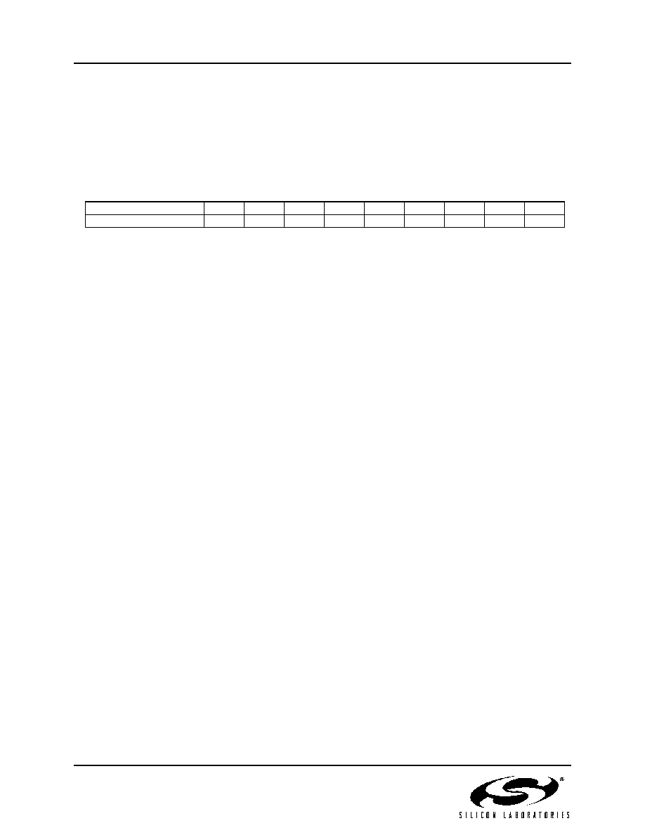
of 109 instructions. The number of instructions versus the system clock cycles required to execute them is as
follows:
Instructions
26
50
5
14
7
3
1
2
1
Clocks to Execute
1
2
2/3
3
3/4
4
4/5
5
8
Programming and Debugging Support
A JTAG-based serial interface is provided for in-system programming of the Flash program memory and
communication with on-chip debug support circuitry. The reprogrammable Flash can also be read and changed a
single byte at a time by the application software using the MOVC and MOVX instructions. This feature allows
program memory to be used for non-volatile data storage as well as updating program code under software control.
The on-chip debug support circuitry facilitates full speed in-circuit debugging, allowing the setting of hardware
breakpoints and watch points, starting, stopping and single stepping through program execution (including interrupt
service routines), examination of the program’s call stack, and reading/writing the contents of registers and memory.
This method of on-chip debugging is completely non-intrusive and non-invasive, requiring no RAM, Stack, timers,
or other on-chip resources.
The CIP-51 is supported by development tools from Silicon Laboratories and third party vendors. Silicon Labs
provides an integrated development environment (IDE) including editor, macro assembler, debugger and
programmer. The IDE’s debugger and programmer interface to the CIP-51 via its JTAG interface to provide fast
and efficient in-system device programming and debugging. Third party macro assemblers and C compilers are also
available.
8.1.
INSTRUCTION SET
The instruction set of the CIP-51 System Controller is fully compatible with the standard MCS-51 instruction set.
Standard 8051 development tools can be used to develop software for the CIP-51. All CIP-51 instructions are the
binary and functional equivalent of their MCS-51 counterparts, including opcodes, addressing modes and effect
on PSW flags. However, instruction timing is different than that of the standard 8051.
8.1.1.
Instruction and CPU Timing
In many 8051 implementations, a distinction is made between machine cycles and clock cycles, with machine cycles
varying from 2 to 12 clock cycles in length. However, the CIP-51 implementation is based solely on clock cycle
timing. All instruction timings are specified in terms of clock cycles.
Due to the pipelined architecture of the CIP-51, most instructions execute in the same number of clock cycles as
there are program bytes in the instruction. Conditional branch instructions take one less clock cycle to complete
when the branch is not taken as opposed to when the branch is taken. Table 8.1 is the CIP-51 Instruction Set
Summary, which includes the mnemonic, number of bytes, and number of clock cycles for each instruction.
8.1.2.
MOVX Instruction and Program Memory
The MOVX instruction is typically used to access external data memory. In the CIP-51, the MOVX instruction can
access the on-chip program memory space implemented as reprogrammable Flash memory using the control bits in
the PSCTL register (see Figure 9.1). This feature provides a mechanism for the CIP-51 to update program code and
use the program memory space for non-volatile data storage. MOVX is still used to read/write this external RAM
with the PSCTL register configured for accessing the external data memory space. Refer to Section 9 (Flash
Memory) for further details.
45
Rev. 1.2
相关PDF资料 |
PDF描述 |
|---|---|
| DSPIC33EP256MU814-I/PL | IC DSC 16BIT 256KB 144LQFP |
| 106457-7 | Z-PACK/A SPACER 1,9 |
| 106458-5 | Z-PACK/B SPACER 1,5 |
| PIC32MX675F512L-80I/PF | IC MCU 32BIT 512KB FLASH 100TQFP |
| 106457-2 | Z-PACK/A SPACER 0,9 |
相关代理商/技术参数 |
参数描述 |
|---|---|
| C8051F018-GQ | 功能描述:8位微控制器 -MCU 16KB 10ADC 64P MCU RoHS:否 制造商:Silicon Labs 核心:8051 处理器系列:C8051F39x 数据总线宽度:8 bit 最大时钟频率:50 MHz 程序存储器大小:16 KB 数据 RAM 大小:1 KB 片上 ADC:Yes 工作电源电压:1.8 V to 3.6 V 工作温度范围:- 40 C to + 105 C 封装 / 箱体:QFN-20 安装风格:SMD/SMT |
| C8051F018-GQR | 功能描述:8位微控制器 -MCU 16KB 10ADC 64Pin MCU Tape and Reel RoHS:否 制造商:Silicon Labs 核心:8051 处理器系列:C8051F39x 数据总线宽度:8 bit 最大时钟频率:50 MHz 程序存储器大小:16 KB 数据 RAM 大小:1 KB 片上 ADC:Yes 工作电源电压:1.8 V to 3.6 V 工作温度范围:- 40 C to + 105 C 封装 / 箱体:QFN-20 安装风格:SMD/SMT |
| C8051F018R | 功能描述:8位微控制器 -MCU C+-10Bit/64Pin RoHS:否 制造商:Silicon Labs 核心:8051 处理器系列:C8051F39x 数据总线宽度:8 bit 最大时钟频率:50 MHz 程序存储器大小:16 KB 数据 RAM 大小:1 KB 片上 ADC:Yes 工作电源电压:1.8 V to 3.6 V 工作温度范围:- 40 C to + 105 C 封装 / 箱体:QFN-20 安装风格:SMD/SMT |
| C8051F019 | 功能描述:8位微控制器 -MCU 16KB 10ADC RoHS:否 制造商:Silicon Labs 核心:8051 处理器系列:C8051F39x 数据总线宽度:8 bit 最大时钟频率:50 MHz 程序存储器大小:16 KB 数据 RAM 大小:1 KB 片上 ADC:Yes 工作电源电压:1.8 V to 3.6 V 工作温度范围:- 40 C to + 105 C 封装 / 箱体:QFN-20 安装风格:SMD/SMT |
| C8051F019-GQ | 功能描述:8位微控制器 -MCU 16KB 10ADC 48P MCU RoHS:否 制造商:Silicon Labs 核心:8051 处理器系列:C8051F39x 数据总线宽度:8 bit 最大时钟频率:50 MHz 程序存储器大小:16 KB 数据 RAM 大小:1 KB 片上 ADC:Yes 工作电源电压:1.8 V to 3.6 V 工作温度范围:- 40 C to + 105 C 封装 / 箱体:QFN-20 安装风格:SMD/SMT |
发布紧急采购,3分钟左右您将得到回复。