- 您现在的位置:买卖IC网 > PDF目录17089 > C8051F410-TB (Silicon Laboratories Inc)BOARD PROTOTYPING W/C8051F410 PDF资料下载
参数资料
| 型号: | C8051F410-TB |
| 厂商: | Silicon Laboratories Inc |
| 文件页数: | 218/270页 |
| 文件大小: | 0K |
| 描述: | BOARD PROTOTYPING W/C8051F410 |
| 标准包装: | 1 |
| 类型: | MCU |
| 适用于相关产品: | C8051F410 |
| 所含物品: | 板 |
第1页第2页第3页第4页第5页第6页第7页第8页第9页第10页第11页第12页第13页第14页第15页第16页第17页第18页第19页第20页第21页第22页第23页第24页第25页第26页第27页第28页第29页第30页第31页第32页第33页第34页第35页第36页第37页第38页第39页第40页第41页第42页第43页第44页第45页第46页第47页第48页第49页第50页第51页第52页第53页第54页第55页第56页第57页第58页第59页第60页第61页第62页第63页第64页第65页第66页第67页第68页第69页第70页第71页第72页第73页第74页第75页第76页第77页第78页第79页第80页第81页第82页第83页第84页第85页第86页第87页第88页第89页第90页第91页第92页第93页第94页第95页第96页第97页第98页第99页第100页第101页第102页第103页第104页第105页第106页第107页第108页第109页第110页第111页第112页第113页第114页第115页第116页第117页第118页第119页第120页第121页第122页第123页第124页第125页第126页第127页第128页第129页第130页第131页第132页第133页第134页第135页第136页第137页第138页第139页第140页第141页第142页第143页第144页第145页第146页第147页第148页第149页第150页第151页第152页第153页第154页第155页第156页第157页第158页第159页第160页第161页第162页第163页第164页第165页第166页第167页第168页第169页第170页第171页第172页第173页第174页第175页第176页第177页第178页第179页第180页第181页第182页第183页第184页第185页第186页第187页第188页第189页第190页第191页第192页第193页第194页第195页第196页第197页第198页第199页第200页第201页第202页第203页第204页第205页第206页第207页第208页第209页第210页第211页第212页第213页第214页第215页第216页第217页当前第218页第219页第220页第221页第222页第223页第224页第225页第226页第227页第228页第229页第230页第231页第232页第233页第234页第235页第236页第237页第238页第239页第240页第241页第242页第243页第244页第245页第246页第247页第248页第249页第250页第251页第252页第253页第254页第255页第256页第257页第258页第259页第260页第261页第262页第263页第264页第265页第266页第267页第268页第269页第270页
Rev. 1.1
51
C8051F410/1/2/3
5.
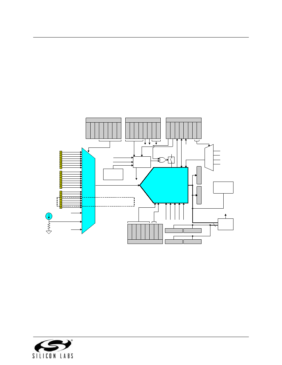
12-Bit ADC (ADC0)
The ADC0 subsystem for the C8051F41x consists of an analog multiplexer (AMUX0) with 27 total input
selections, and a 200 ksps, 12-bit successive-approximation-register ADC with integrated track-and-hold,
programmable window detector, and hardware accumulator. The ADC0 subsystem has a special
Burst
Mode which can automatically enable ADC0, capture and accumulate samples, then place ADC0 in a low
power shutdown mode without CPU intervention. The AMUX0, data conversion modes, and window detec-
tor are all configurable under software control via the Special Function Registers shown in Figure 5.1.
ADC0 inputs are single-ended and may be configured to measure P0.0-P2.7, the Temperature Sensor out-
put, VDD, or GND with respect to GND. ADC0 is enabled when the AD0EN bit in the ADC0 Control register
(ADC0CN) is set to logic 1, or when performing conversions in Burst Mode. ADC0 is in low power shut-
down when AD0EN is logic 0 and no Burst Mode conversions are taking place.
12-Bit
SAR
ADC
RE
F
FCLK
ADC0H
32
ADC0CN
AD0CM0
AD0CM1
AD0LJS
T
AD
0
WIN
T
AD0B
U
S
Y
AD
0IN
T
BURS
T
E
N
AD0
E
N
Timer 2 Overflow
Start
Conversion
00
AD0BUSY (W)
VDD
ADC0LTH
AD0WINT
27-to-1
AMUX
VDD
P0.0
P0.7
01
10
11
CNVSTR Input
Window
Compare
Logic
P1.0
P1.7
Timer 3 Overflow
ADC0LTL
ADC0GTH ADC0GTL
ADC0L
ADC0MX
ADC0MX4
ADC0MX3
ADC0MX2
ADC0MX1
ADC0MX0
P2.0
P2.3-P2.6 available on
‘F410/2
P2.7
GND
Temp Sensor
ADC0CF
AD0RPT
0
AD0RPT
1
AD0S
C0
AD0S
C1
AD0S
C2
AD0S
C3
AD0S
C4
ADC0TK
AD0PWR3
AD0PWR2
AD0PWR1
AD0PWR0
AD0T
M
1
AD0T
M
0
AD0
T
K1
AD0
T
K0
Burst Mode
Logic
AD0PO
S
T
AD0P
R
E
AD0
T
M
1:0
Accumulator
Start
Conversion
Burst Mode
Oscillator
25 MHz Max
SYSCLK
FC
LK
Figure 5.1. ADC0 Functional Block Diagram
5.1.
Analog Multiplexer
AMUX0 selects the input channel to the ADC. Any of the following may be selected as an input: P0.0-P2.7,
the on-chip temperature sensor, the core power supply (VDD), or ground (GND). ADC0 is single-ended
and all signals measured are with respect to GND. The ADC0 input channels are selected using the
ADC0MX register as described in SFR Definition 5.1.
Important Note About ADC0 Input Configuration: Port pins selected as ADC0 inputs should be config-
ured as analog inputs and should be skipped by the Digital Crossbar. To configure a Port pin for analog
input, set to ‘0’ the corresponding bit in register PnMDIN (for n = 0,1,2) and write a ‘1’ in the corresponding
Port Latch register Pn (for n = 0,1,2). To force the Crossbar to skip a Port pin, set to ‘1’ the corresponding
bit in register PnSKIP (for n = 0,1,2). See Section “18. Port Input/Output” on page 147 for more Port I/O
configuration details.
相关PDF资料 |
PDF描述 |
|---|---|
| EBC25DRYS | CONN EDGECARD 50POS DIP .100 SLD |
| SDR-80-89 | SCOTCH CODE REFILL # 80-89 |
| ECC19DREH-S13 | CONN EDGECARD 38POS .100 EXTEND |
| SDR-U | SCOTCH CODE REFILL U |
| DM163022 | BOARD DEMO PICDEM-2 PLUS |
相关代理商/技术参数 |
参数描述 |
|---|---|
| C8051F410-TB-K | 功能描述:BOARD PROTOTYPING W/C8051F410 制造商:silicon labs 系列:- 零件状态:在售 板类型:评估平台 类型:MCU 8-位 核心处理器:8051 操作系统:- 平台:- 配套使用产品/相关产品:C8051F41x 安装类型:固定 内容:板 标准包装:1 |
| C8051F411 | 制造商:SILABS 制造商全称:SILABS 功能描述:2.0 V, 32/16 kB Flash, smaRTClock, 12-bit ADC |
| C8051F411EK | 功能描述:开发板和工具包 - 8051 EVAL KIT FOR C8051F411 RoHS:否 制造商:Silicon Labs 产品:Development Kits 工具用于评估:C8051F960, Si7005 核心: 接口类型:USB 工作电源电压: |
| C8051F411-GM | 功能描述:8位微控制器 -MCU 50 MIPS 32KB 12ADC RTCLOCK 28 PIN MCU RoHS:否 制造商:Silicon Labs 核心:8051 处理器系列:C8051F39x 数据总线宽度:8 bit 最大时钟频率:50 MHz 程序存储器大小:16 KB 数据 RAM 大小:1 KB 片上 ADC:Yes 工作电源电压:1.8 V to 3.6 V 工作温度范围:- 40 C to + 105 C 封装 / 箱体:QFN-20 安装风格:SMD/SMT |
| C8051F411-GMR | 功能描述:8位微控制器 -MCU 50 MIPS 32KB 12ADC RTCLOCK 28 PIN MCU RoHS:否 制造商:Silicon Labs 核心:8051 处理器系列:C8051F39x 数据总线宽度:8 bit 最大时钟频率:50 MHz 程序存储器大小:16 KB 数据 RAM 大小:1 KB 片上 ADC:Yes 工作电源电压:1.8 V to 3.6 V 工作温度范围:- 40 C to + 105 C 封装 / 箱体:QFN-20 安装风格:SMD/SMT |
发布紧急采购,3分钟左右您将得到回复。