- 您现在的位置:买卖IC网 > PDF目录366628 > C9706AY ST92141 - 8/16 BIT MCU FOR 3-PHASE AC MOTOR CONTROL PDF资料下载
参数资料
| 型号: | C9706AY |
| 英文描述: | ST92141 - 8/16 BIT MCU FOR 3-PHASE AC MOTOR CONTROL |
| 中文描述: | CPU系统时钟发生器| SSOP封装| 48PIN |塑料 |
| 文件页数: | 7/19页 |
| 文件大小: | 248K |
| 代理商: | C9706AY |
C9706
Clock Generator for VIA VT8371/Athlon (K7) Chipset Systems
Approved Product
Cypress Semiconductor Corporation
525 Los Coches St.
Milpitas, CA 95035. Tel: 408-263-6300, Fax: 408-263-6571
http://www.cypress.com
Document#: 38-07041 Rev. **
05/02/2001
Page 7 of 19
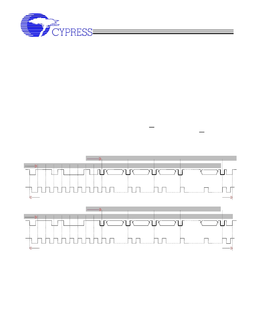
2-Wire SMBus Control Interface
The 2-wire control interface implements a read/write slave only interface according to SMBus specification. (see fig6,
page 7) . The device can be read back by using standard SMBus command bytes. Sub-addressing is not supported,
thus all preceding bytes must be sent in order to change one of the control bytes. The 2-wire control interface allows
each clock output to be individually enabled or disabled. 100 Kbits/second (standard mode) data transfer is supported.
During normal data transfer, the SDATA signal only changes when the SCLK signal is low, and is stable when SCLK is
high. There are two exceptions to this. A high to low transition on SDATA while SCLK is high is used to indicate the
start of a data transfer cycle. A low to high transition on SDATA while SCLK is high indicates the end of a data transfer
cycle. Data is always sent as complete 8-bit bytes, after which an “acknowledge” is generated. The first byte of a
transfer cycle is a 7-bit address with a Read/Write bit (R/W#) as the LSB. R/W# = 1 in read mode. R/W# = 0 in write
mode.
The device will respond to writes to 10 bytes (max) of data to address
D2
by generating the “acknowledge” (low) signal
on the SDATA wire following reception of each byte. If the device should be read then an address
D3
must be sent.
Data is transferred MSB first at a max rate of 100kbits/S.
The device will not respond to any other control interface conditions, and previously set control registers are retained.
START CONDITION
Transmit
Receive
STOP CONDITION
START CONDITION
Transmit
Receiv
STOP CONDITION
1
8
ACK
MSB
0
0
0
SDATA
0
1
LSB
COMMAND BYTE
1
SCLK
1
BYTE N
8
8
8
BYTE 0
BYTE COUNT
ACK
ACK
ACK
ACK
(Don't Care)
(Don't Care)
(Valid)
(Valid)
Fig.7a
(WRITE)
(Valid)
SDATA
1
0
(Valid)
0
1
1
8
BYTE N
(Valid)
BYTE COUNT
SCLK
LSB
ACK
8
ACK
ACK
8
0
BYTE1
1
ACK
ACK
MSB
8
1
(Valid)
BYTE 0
Fig.7b (READ)
Figure 7
SMBus Communications Waveforms
相关PDF资料 |
PDF描述 |
|---|---|
| C9726AY | ST92141 - 8/16 BIT MCU FOR 3-PHASE AC MOTOR CONTROL |
| C9801CY | Hex buffer |
| C9805CYB | Quad line receivers |
| C9811X2AYB | Up to 5A ULDO linear regulator |
| C9812DYB | Up to 5A ULDO linear regulator |
相关代理商/技术参数 |
参数描述 |
|---|---|
| C9714 | 制造商:未知厂家 制造商全称:未知厂家 功能描述:100 MHz Clock Generator with SSCG and Power Management for Mobile Application |
| C9714AT | 制造商:未知厂家 制造商全称:未知厂家 功能描述:100 MHz Clock Generator with SSCG and Power Management for Mobile Application |
| C9714AY | 制造商:未知厂家 制造商全称:未知厂家 功能描述:100 MHz Clock Generator with SSCG and Power Management for Mobile Application |
| C9716J | 制造商:未知厂家 制造商全称:未知厂家 功能描述:100 MHz Clock Generator with SSCG and Power Management for Mobile Application |
| C9716JT | 制造商:未知厂家 制造商全称:未知厂家 功能描述:100 MHz Clock Generator with SSCG and Power Management for Mobile Application |
发布紧急采购,3分钟左右您将得到回复。