参数资料
| 型号: | CAT25640VI-GT3 |
| 厂商: | ON Semiconductor |
| 文件页数: | 6/19页 |
| 文件大小: | 0K |
| 描述: | IC EEPROM 64KBIT 10MHZ 8SOIC |
| 标准包装: | 1 |
| 格式 - 存储器: | EEPROMs - 串行 |
| 存储器类型: | EEPROM |
| 存储容量: | 64K (8K x 8) |
| 速度: | 20MHz |
| 接口: | SPI 3 线串行 |
| 电源电压: | 1.8 V ~ 5.5 V |
| 工作温度: | -40°C ~ 85°C |
| 封装/外壳: | 8-SOIC(0.154",3.90mm 宽) |
| 供应商设备封装: | 8-SOIC |
| 包装: | 标准包装 |
| 其它名称: | CAT25640VI-GT3OSDKR |
�� �
�
�CAT25640�
�Pin� Description�
�SI:� The� serial� data� input� pin� accepts� op� ?� codes,� addresses�
�and� data.� In� SPI� modes� (0,0)� and� (1,1)� input� data� is� latched�
�on� the� rising� edge� of� the� SCK� clock� input.�
�SO:� The� serial� data� output� pin� is� used� to� transfer� data� out� of�
�the� device.� In� SPI� modes� (0,0)� and� (1,1)� data� is� shifted� out�
�on� the� falling� edge� of� the� SCK� clock.�
�SCK:� The� serial� clock� input� pin� accepts� the� clock� provided�
�by� the� host� and� used� for� synchronizing� communication�
�between� host� and� CAT25640.�
�CS:� The� chip� select� input� pin� is� used� to� enable/disable� the�
�CAT25640.� When� CS� is� high,� the� SO� output� is� tri� ?� stated� (high�
�impedance)� and� the� device� is� in� Standby� Mode� (unless� an�
�internal� write� operation� is� in� progress).� Every� communication�
�session� between� host� and� CAT25640� must� be� preceded� by� a�
�Functional� Description�
�The� CAT25640� device� supports� the� Serial� Peripheral�
�Interface� (SPI)� bus� protocol,� modes� (0,0)� and� (1,1).� The�
�device� contains� an� 8� ?� bit� instruction� register.� The� instruction�
�set� and� associated� op� ?� codes� are� listed� in� Table� 9.�
�Reading� data� stored� in� the� CAT25640� is� accomplished� by�
�simply� providing� the� READ� command� and� an� address.�
�Writing� to� the� CAT25640,� in� addition� to� a� WRITE�
�command,� address� and� data,� also� requires� enabling� the�
�device� for� writing� by� first� setting� certain� bits� in� a� Status�
�Register,� as� will� be� explained� later.�
�After� a� high� to� low� transition� on� the� CS� input� pin,� the�
�CAT25640� will� accept� any� one� of� the� six� instruction�
�op� ?� codes� listed� in� Table� 9� and� will� ignore� all� other� possible�
�8� ?� bit� combinations.� The� communication� protocol� follows�
�the� timing� from� Figure� 2.�
�high� to� low� transition� and� concluded� with� a� low� to� high�
�transition� of� the� CS� input.�
�WP:� The� write� protect� input� pin� will� allow� all� write�
�operations� to� the� device� when� held� high.� When� WP� pin� is�
�Table� 9.� INSTRUCTION� SET�
�Instruction� Op� ?� code�
�WREN� 0000� 0110�
�Operation�
�Enable� Write� Operations�
�tied� low� and� the� WPEN� bit� in� the� Status� Register� (refer� to�
�Status� Register� description,� later� in� this� Data� Sheet)� is� set� to�
�“1”,� writing� to� the� Status� Register� is� disabled.�
�HOLD:� The� HOLD� input� pin� is� used� to� pause� transmission�
�between� host� and� CAT25640,� without� having� to� retransmit�
�the� entire� sequence� at� a� later� time.� To� pause,� HOLD� must� be�
�WRDI�
�RDSR�
�WRSR�
�READ�
�WRITE�
�0000� 0100�
�0000� 0101�
�0000� 0001�
�0000� 0011�
�0000� 0010�
�Disable� Write� Operations�
�Read� Status� Register�
�Write� Status� Register�
�Read� Data� from� Memory�
�Write� Data� to� Memory�
�taken� low� and� to� resume� it� must� be� taken� back� high,� with� the�
�SCK� input� low� during� both� transitions.� When� not� used� for�
�pausing,� the� HOLD� input� should� be� tied� to� V� CC� ,� either�
�directly� or� through� a� resistor.�
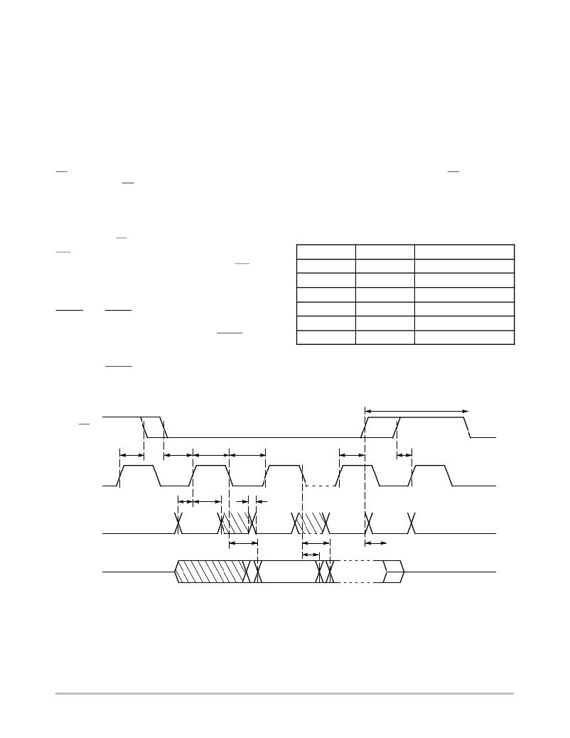
�t� CS�
�CS�
�t� CNH�
�t� CSS�
�t� WH�
�t� WL�
�t� CSH�
�t� CNS�
�SCK�
�SI�
�t� SU�
�t� H�
�VALID�
�IN�
�t� RI�
�t� FI�
�t� V�
�t� HO�
�t� V�
�t� DIS�
�SO�
�HI� ?� Z�
�VALID�
�OUT�
�HI� ?� Z�
�Figure� 2.� Synchronous� Data� Timing�
�http://onsemi.com�
�6�
�相关PDF资料 |
PDF描述 |
|---|---|
| 396-020-522-802 | CARD EDGE 20POS DL .125X.250 BLK |
| MPC8572ELPXARLD | MPU POWERQUICC III 1023-PBGA |
| 396-020-522-204 | CARD EDGE 20POS DL .125X.250 BLK |
| 396-020-522-202 | CARD EDGE 20POS DL .125X.250 BLK |
| MPC8572ECVTAULB | MPU POWERQUICC III 1023-PBGA |
相关代理商/技术参数 |
参数描述 |
|---|---|
| CAT25640VP2I-GT3 | 功能描述:电可擦除可编程只读存储器 64K SPI Serial RoHS:否 制造商:Atmel 存储容量:2 Kbit 组织:256 B x 8 数据保留:100 yr 最大时钟频率:1000 KHz 最大工作电流:6 uA 工作电源电压:1.7 V to 5.5 V 最大工作温度:+ 85 C 安装风格:SMD/SMT 封装 / 箱体:SOIC-8 |
| CAT25640VP2IGT3E | 制造商:ON Semiconductor 功能描述: |
| CAT25640YE-GE | 制造商:ON Semiconductor 功能描述: |
| CAT25640YI-G | 功能描述:电可擦除可编程只读存储器 CMOS 电可擦除可编程只读存储器 RoHS:否 制造商:Atmel 存储容量:2 Kbit 组织:256 B x 8 数据保留:100 yr 最大时钟频率:1000 KHz 最大工作电流:6 uA 工作电源电压:1.7 V to 5.5 V 最大工作温度:+ 85 C 安装风格:SMD/SMT 封装 / 箱体:SOIC-8 |
| CAT25640YI-GT3 | 功能描述:电可擦除可编程只读存储器 (8192x8) 64K 1.8-5.5 RoHS:否 制造商:Atmel 存储容量:2 Kbit 组织:256 B x 8 数据保留:100 yr 最大时钟频率:1000 KHz 最大工作电流:6 uA 工作电源电压:1.7 V to 5.5 V 最大工作温度:+ 85 C 安装风格:SMD/SMT 封装 / 箱体:SOIC-8 |
发布紧急采购,3分钟左右您将得到回复。