参数资料
| 型号: | CAT93C86VI-GT3 |
| 厂商: | ON Semiconductor |
| 文件页数: | 4/10页 |
| 文件大小: | 0K |
| 描述: | IC EEPROM 16KBIT 3MHZ 8SOIC |
| 标准包装: | 1 |
| 格式 - 存储器: | EEPROMs - 串行 |
| 存储器类型: | EEPROM |
| 存储容量: | 16K(2K x 8 或 1K x 16) |
| 速度: | 3MHz |
| 接口: | Microwire 3 线串行 |
| 电源电压: | 2.5 V ~ 5.5 V |
| 工作温度: | -40°C ~ 85°C |
| 封装/外壳: | 8-SOIC(0.154",3.90mm 宽) |
| 供应商设备封装: | 8-SOIC |
| 包装: | 标准包装 |
| 产品目录页面: | 807 (CN2011-ZH PDF) |
| 其它名称: | CAT93C86VI-GT3DKR |
�� �
�
�CAT93C86�
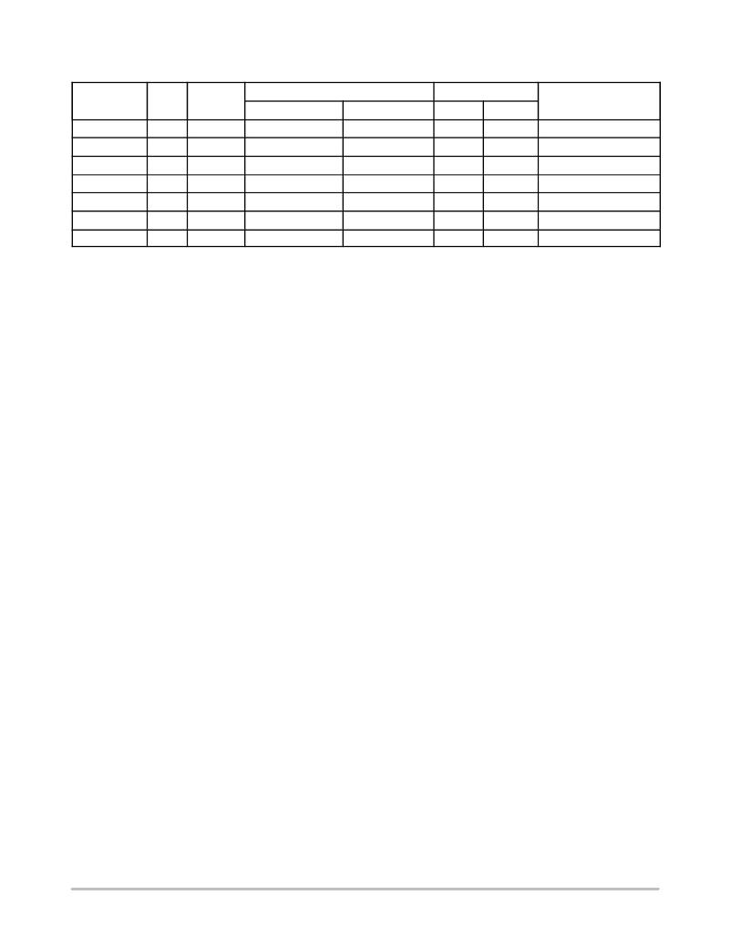
�Table� 8.� INSTRUCTION� SET�
�Start�
�Address�
�Data�
�Instruction�
�READ�
�ERASE�
�WRITE�
�EWEN�
�EWDS�
�ERAL�
�WRAL�
�Bit�
�1�
�1�
�1�
�1�
�1�
�1�
�1�
�Opcode�
�10�
�11�
�01�
�00�
�00�
�00�
�00�
�x8�
�A10� ?� A0�
�A10� ?� A0�
�A10� ?� A0�
�11XXXXXXXXX�
�00XXXXXXXXX�
�10XXXXXXXXX�
�01XXXXXXXXX�
�x16�
�A9� ?� A0�
�A9� ?� A0�
�A9� ?� A0�
�11XXXXXXXX�
�00XXXXXXXX�
�10XXXXXXXX�
�01XXXXXXXX�
�x8�
�D7� ?� D0�
�D7� ?� D0�
�x16�
�D15� ?� D0�
�D15� ?� D0�
�Comments�
�Read� Address� AN–� A0�
�Clear� Address� AN–� A0�
�Write� Address� AN–� A0�
�Write� Enable�
�Write� Disable�
�Clear� All� Addresses�
�Write� All� Addresses�
�Device� Operation�
�The� CAT93C86� is� a� 16,384� ?� bit� nonvolatile� memory�
�intended� for� use� with� industry� standard� microprocessors.�
�The� CAT93C86� can� be� organized� as� either� registers� of� 16�
�bits� or� 8� bits.� When� organized� as� X16,� seven� 13� ?� bit�
�instructions� control� the� reading,� writing� and� erase�
�operations� of� the� device.� When� organized� as� X8,� seven�
�14� ?� bit� instructions� control� the� reading,� writing� and� erase�
�operations� of� the� device.� The� CAT93C86� operates� on� a�
�single� power� supply� and� will� generate� on� chip,� the� high�
�voltage� required� during� any� write� operation.�
�Instructions,� addresses,� and� write� data� are� clocked� into� the�
�DI� pin� on� the� rising� edge� of� the� clock� (SK).� The� DO� pin� is�
�normally� in� a� high� impedance� state� except� when� reading� data�
�from� the� device,� or� when� checking� the� ready/busy� status�
�after� a� write� operation.�
�The� ready/busy� status� can� be� determined� after� the� start� of�
�a� write� operation� by� selecting� the� device� (CS� high)� and�
�polling� the� DO� pin;� DO� low� indicates� that� the� write�
�operation� is� not� completed,� while� DO� high� indicates� that� the�
�device� is� ready� for� the� next� instruction.� If� necessary,� the� DO�
�pin� may� be� placed� back� into� a� high� impedance� state� during�
�chip� select� by� shifting� a� dummy� “1”� into� the� DI� pin.� The� DO�
�pin� will� enter� the� high� impedance� state� on� the� falling� edge� of�
�the� clock� (SK).� Placing� the� DO� pin� into� the� high� impedance�
�state� is� recommended� in� applications� where� the� DI� pin� and�
�the� DO� pin� are� to� be� tied� together� to� form� a� common� DI/O�
�pin.�
�The� format� for� all� instructions� sent� to� the� device� is� a�
�logical� “1”� start� bit,� a� 2� ?� bit� (or� 4� ?� bit)� opcode,� 10� ?� bit� address�
�(an� additional� bit� when� organized� X8)� and� for� write�
�operations� a� 16� ?� bit� data� field� (8� ?� bit� for� X8� organizations).�
�Read�
�Upon� receiving� a� READ� command� and� an� address�
�(clocked� into� the� DI� pin),� the� DO� pin� of� the� CAT93C86� will�
�come� out� of� the� high� impedance� state� and,� after� sending� an�
�initial� dummy� zero� bit,� will� begin� shifting� out� the� data�
�addressed� (MSB� first).� The� output� data� bits� will� toggle� on�
�the� rising� edge� of� the� SK� clock� and� are� stable� after� the�
�specified� time� delay� (t� PD0� or� t� PD1� ).�
�After� the� initial� data� word� has� been� shifted� out� and� CS�
�remains� asserted� with� the� SK� clock� continuing� to� toggle,� the�
�device� will� automatically� increment� to� the� next� address� and�
�shift� out� the� next� data� word� in� a� sequential� READ� mode.� As�
�long� as� CS� is� continuously� asserted� and� SK� continues� to�
�toggle,� the� device� will� keep� incrementing� to� the� next� address�
�automatically� until� it� reaches� to� the� end� of� the� address� space,�
�then� loops� back� to� address� 0.� In� the� sequential� READ� mode,�
�only� the� initial� data� word� is� preceeded� by� a� dummy� zero� bit.�
�All� subsequent� data� words� will� follow� without� a� dummy�
�zero� bit.�
�Write�
�After� receiving� a� WRITE� command,� address� and� the� data,�
�the� CS� (Chip� Select)� pin� must� be� deselected� for� a� minimum�
�of� t� CSMIN� .� The� falling� edge� of� CS� will� start� the� self� clocking�
�clear� and� data� store� cycle� of� the� memory� location� specified�
�in� the� instruction.� The� clocking� of� the� SK� pin� is� not�
�necessary� after� the� device� has� entered� the� self� clocking�
�mode.� The� ready/busy� status� of� the� CAT93C86� can� be�
�determined� by� selecting� the� device� and� polling� the� DO� pin.�
�Since� this� device� features� Auto� ?� Clear� before� write,� it� is�
�NOT� necessary� to� erase� a� memory� location� before� it� is�
�written� into.�
�Note:� The� Write,� Erase,� Write� all� and� Erase� all� instructions�
�require� PE� =� 1.� If� PE� is� left� floating,� 93C86� is� in� Program�
�Enabled� mode.� For� Write� Enable� and� Write� Disable�
�instruction� PE� =� don’t� care.�
�http://onsemi.com�
�4�
�相关PDF资料 |
PDF描述 |
|---|---|
| M1A3P1000L-FGG256I | IC FPGA M1 1KB FLASH 1M 256FBGA |
| 956-009-010R011 | BACKSHELL 9POS STR SNAP PLAS BLK |
| 10368-12R1-00 | JUNCTION SHELL 68POS METAL |
| M1A3P1000L-FG256I | IC FPGA M1 1KB FLASH 1M 256FBGA |
| EP4CE40F29I7N | IC CYCLONE IV FPGA 40K 780FBGA |
相关代理商/技术参数 |
参数描述 |
|---|---|
| CAT93C86VIG-T3 | 制造商:ON Semiconductor 功能描述:EEPROM Serial-Microwire 16K-bit 2K x 8/1K x 16 2.5V/3.3V/5V 8-Pin SOIC N T/R |
| CAT93C86VI-GT3 | 制造商:ON Semiconductor 功能描述:IC EEPROM 16KBIT SERIAL 3MHZ SOIC-8 |
| CAT93C86VI-GT3-CUT TAPE | 制造商:ON 功能描述:CAT93C Series 16 kb (1kX16) 3 MHz 1.8 to 5.5 V Microwire Serial EEPROM - SOIC-8 |
| CAT93C86VI-TE13 | 制造商:Rochester Electronics LLC 功能描述: 制造商:Catalyst Semiconductor 功能描述: |
| CAT93C86V-TE13 | 功能描述:电可擦除可编程只读存储器 (2048x8)(1024x16)16K RoHS:否 制造商:Atmel 存储容量:2 Kbit 组织:256 B x 8 数据保留:100 yr 最大时钟频率:1000 KHz 最大工作电流:6 uA 工作电源电压:1.7 V to 5.5 V 最大工作温度:+ 85 C 安装风格:SMD/SMT 封装 / 箱体:SOIC-8 |
发布紧急采购,3分钟左右您将得到回复。