参数资料
| 型号: | CP80C86-2Z |
| 厂商: | Intersil |
| 文件页数: | 6/37页 |
| 文件大小: | 0K |
| 描述: | IC CPU 16BIT 5V 8MHZ 40-PDIP |
| 标准包装: | 9 |
| 处理器类型: | 80C86 16-位 |
| 速度: | 8MHz |
| 电压: | 4.5 ~ 5.5V |
| 安装类型: | 通孔 |
| 封装/外壳: | 40-DIP(0.600",15.24mm) |
| 供应商设备封装: | 40-DIP |
| 包装: | 管件 |
第1页第2页第3页第4页第5页当前第6页第7页第8页第9页第10页第11页第12页第13页第14页第15页第16页第17页第18页第19页第20页第21页第22页第23页第24页第25页第26页第27页第28页第29页第30页第31页第32页第33页第34页第35页第36页第37页
14
FN2957.3
January 9, 2009
.
Halt
When a software “HALT” instruction is executed, the
processor indicates that it is entering the “HALT” state in one
of two ways depending upon which mode is strapped. In
minimum mode, the processor issues one ALE with no
qualifying bus control signals. In maximum mode the
processor issues appropriate HALT status on S2, S1, S0 and
the 82C88 bus controller issues one ALE. The 80C86 will not
leave the “HALT” state when a local bus “hold” is entered
while in “HALT”. In this case, the processor reissues the
HALT indicator at the end of the local bus hold. An NMI or
interrupt request (when interrupts enabled) or RESET will
force the 80C86 out of the “HALT” state.
Read/Modify/Write (Semaphore)
Operations Via Lock
The LOCK status information is provided by the processor
when consecutive bus cycles are required during the execution
of an instruction. This gives the processor the capability of
performing read/modify/write operations on memory (via the
Exchange Register With Memory instruction, for example)
without another system bus master receiving intervening
memory cycles. This is useful in multiprocessor system
configurations to accomplish “test and set lock” operations. The
LOCK signal is activated (forced LOW) in the clock cycle
following decoding of the software “LOCK” prefix instruction. It
is deactivated at the end of the last bus cycle of the instruction
following the “LOCK” prefix instruction. While LOCK is active a
request on a RQ/GT pin will be recorded and then honored at
the end of the LOCK.
External Synchronization Via TEST
As an alternative to interrupts, the 80C86 provides a single
software-testable input pin (TEST). This input is utilized by
executing a WAIT instruction. The single WAIT instruction is
repeatedly executed until the TEST input goes active (LOW).
The execution of WAIT does not consume bus cycles once
the queue is full.
If a local bus request occurs during WAIT execution, the
80C86 three-states all output drivers while inputs and I/O
pins are held at valid logic levels by internal bus-hold
circuits. If interrupts are enabled, the 80C86 will recognize
interrupts and process them when it regains control of the
bus. The WAIT instruction is then refetched, and
re-executed.
TABLE 4. 80C86 REGISTER
Basic System Timing
Typical system configurations for the processor operating in
minimum mode and in maximum mode are shown in
MN/MX pin is strapped to VCC and the processor emits bus
control signals (e.g. RD, WR, etc.) directly. In maximum
mode, the MN/MX pin is strapped to GND and the processor
emits coded status information which the 82C88 bus
controller uses to generate MULTIBUS compatible bus
control signals. Figure 3 shows the signal timing
relationships.
System Timing - Minimum System
The read cycle begins in t1 with the assertion of the Address
Latch Enable (ALE) signal. The trailing (low-going) edge of
this signal is used to latch the address information, which is
valid on the address/data bus (AD0-AD15) at this time, into
the 82C82/82C83 latch. The BHE and A0 signals address
the low, high or both bytes. From t1 to t4 the M/lO signal
indicates a memory or I/O operation. At t2, the address is
removed from the address/data bus and the bus is held at
the last valid logic state by internal bus hold devices. The
read control signal is also asserted at t2. The read (RD)
signal causes the addressed device to enable its data bus
drivers to the local bus. Some time later, valid data will be
available on the bus and the addressed device will drive the
READY line HIGH. When the processor returns the read
signal to a HIGH level, the addressed device will again
three-state its bus drivers. If a transceiver (82C86/82C87) is
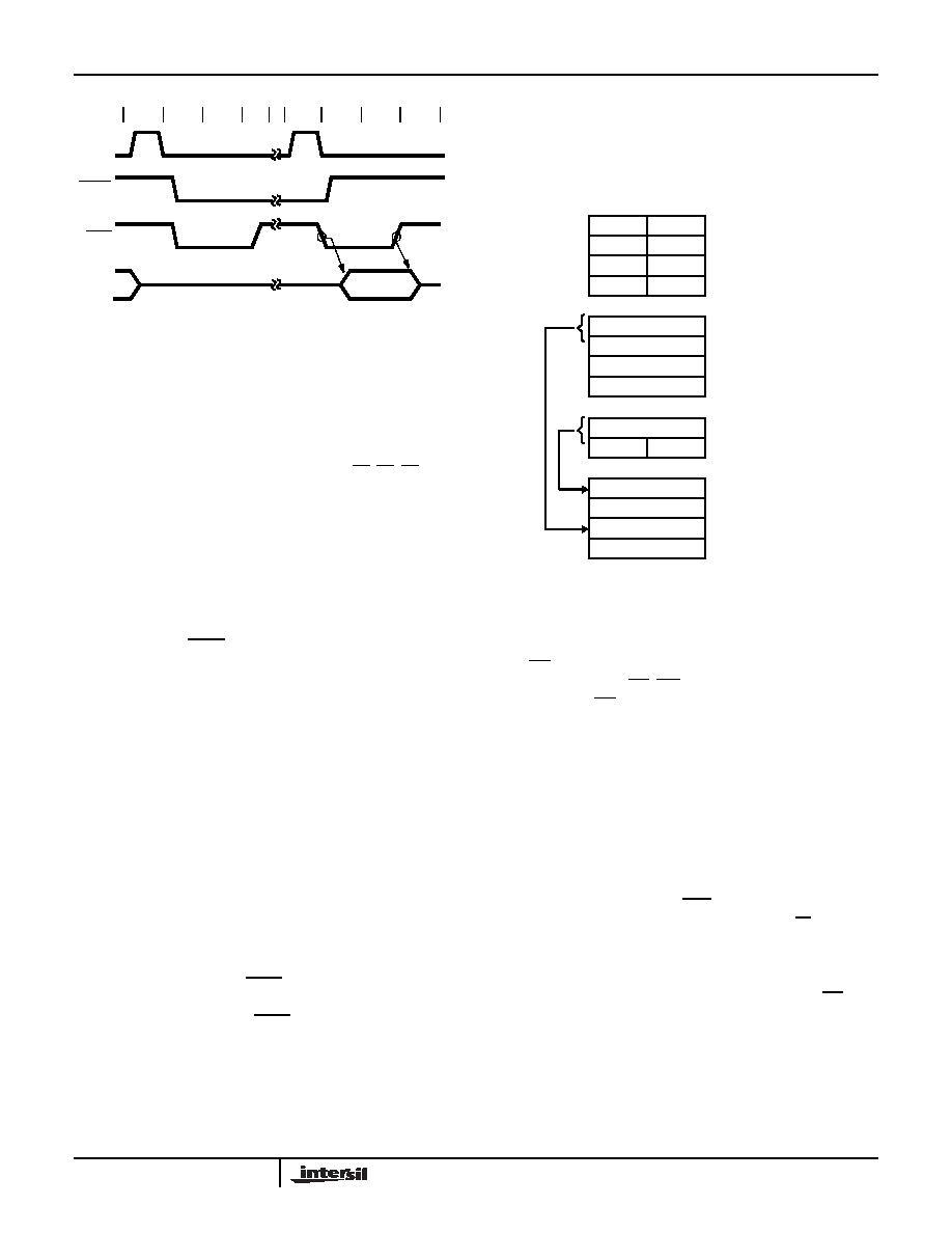
ALE
LOCK
INTA
AD0-
FLOAT
TYPE
AD15
t1
t2
t3
t4 TI
t1
t2
t3
t4
VECTOR
FIGURE 5. INTERRUPT ACKNOWLEDGE SEQUENCE
AH
AL
BH
CH
DH
BL
CL
DL
SP
BP
SI
DI
IP
FLAGSH
FLAGSL
CS
DS
SS
ES
AX
BX
CX
DX
ACCUMULATOR
BASE
COUNT
DATA
STACK POINTER
BASE POINTER
SOURCE INDEX
DESTINATION INDEX
INSTRUCTION POINTER
STATUS FLAG
CODE SEGMENT
DATA SEGMENT
STACK SEGMENT
EXTRA SEGMENT
80C86
相关PDF资料 |
PDF描述 |
|---|---|
| CP82C50A-5Z | IC ASYNC COMM ELEMENT UART 40DIP |
| CP82C89 | IC ARBITER BUS 5V 8MHZ 20-DIP |
| CPC1465D | IC DC TERMINATION 16-SOIC |
| CPC1465M | IC SHDSL/ISDN DC TERM 16MLP |
| CPC2400E | MODULE MODEM 2400BAUD EMBEDDEDED |
相关代理商/技术参数 |
参数描述 |
|---|---|
| CP80C86R2489 | 制造商:Rochester Electronics LLC 功能描述:- Bulk 制造商:Harris Corporation 功能描述: |
| CP80C88 | 功能描述:微处理器 - MPU CPU 8/16BIT 5V 5MHZ 40PDIP COM RoHS:否 制造商:Atmel 处理器系列:SAMA5D31 核心:ARM Cortex A5 数据总线宽度:32 bit 最大时钟频率:536 MHz 程序存储器大小:32 KB 数据 RAM 大小:128 KB 接口类型:CAN, Ethernet, LIN, SPI,TWI, UART, USB 工作电源电压:1.8 V to 3.3 V 最大工作温度:+ 85 C 安装风格:SMD/SMT 封装 / 箱体:FBGA-324 |
| CP80C88-2 | 功能描述:微处理器 - MPU CPU 8/16BIT 5V 8MHZ 40PDIP COM RoHS:否 制造商:Atmel 处理器系列:SAMA5D31 核心:ARM Cortex A5 数据总线宽度:32 bit 最大时钟频率:536 MHz 程序存储器大小:32 KB 数据 RAM 大小:128 KB 接口类型:CAN, Ethernet, LIN, SPI,TWI, UART, USB 工作电源电压:1.8 V to 3.3 V 最大工作温度:+ 85 C 安装风格:SMD/SMT 封装 / 箱体:FBGA-324 |
| CP80C88-2Z | 功能描述:IC PWM CONTROLLER RoHS:是 类别:集成电路 (IC) >> 嵌入式 - 微处理器 系列:- 标准包装:40 系列:MPC83xx 处理器类型:32-位 MPC83xx PowerQUICC II Pro 特点:- 速度:267MHz 电压:0.95 V ~ 1.05 V 安装类型:表面贴装 封装/外壳:516-BBGA 裸露焊盘 供应商设备封装:516-PBGAPGE(27x27) 包装:托盘 |
| CP80C88R2489 | 制造商:Rochester Electronics LLC 功能描述:- Bulk |
发布紧急采购,3分钟左右您将得到回复。