- 您现在的位置:买卖IC网 > PDF目录170207 > CS5361GD16 (ON SEMICONDUCTOR) 2 A BATTERY CHARGE CONTROLLER, 635 kHz SWITCHING FREQ-MAX, PDSO16 PDF资料下载
参数资料
| 型号: | CS5361GD16 |
| 厂商: | ON SEMICONDUCTOR |
| 元件分类: | 稳压器 |
| 英文描述: | 2 A BATTERY CHARGE CONTROLLER, 635 kHz SWITCHING FREQ-MAX, PDSO16 |
| 封装: | SOIC-16 |
| 文件页数: | 5/15页 |
| 文件大小: | 120K |
| 代理商: | CS5361GD16 |
CS5361
http://onsemi.com
1243
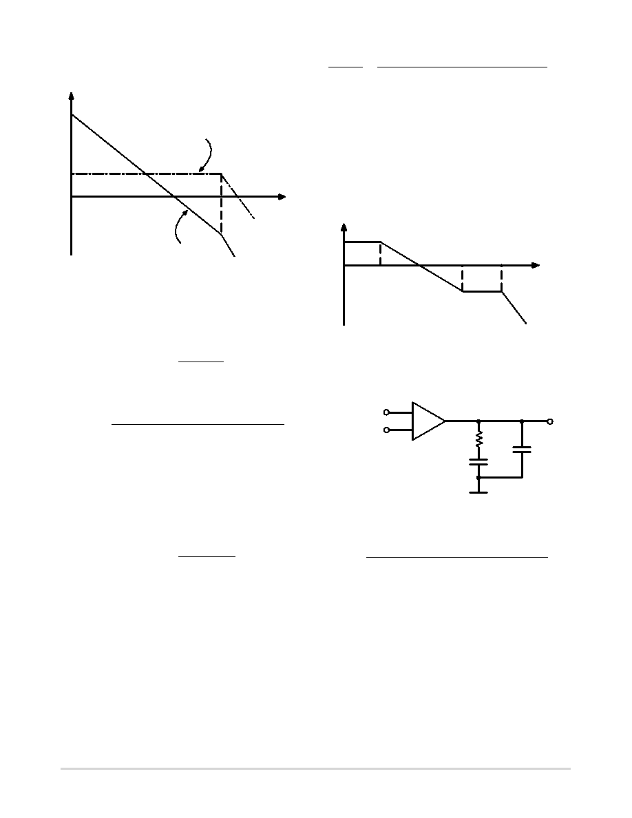
closed loop control–to–output transfer function without and
with compensation is shown in Figure 5.
Figure 5. Bode Plot of Control–to–Output
Transfer Function
dB
With Compensation
–1
–2
f
–3
Without Compensation
fs/2
If a transconductance amplifier is used as the error
amplifier, the integrator pole can be implemented by
connecting a capacitor from the amplifier output to the
ground. The compensation gain is given by:
FC(s) +
G
(sCCOMP)
(63)
where G is the transconductance of the amplifier.
The total loop gain is
T(s)
+
G
RI
sCCOMP 1.0 ) s (wnQ) ) s2 wn2
(64)
The value of the compensation capacitor CCOMP can be
calculated if the crossover frequency is known. Generally,
the crossover frequency should be chosen well below the
switching frequency.
We can choose
fCO + 1 6
fS
So
CCOMP +
G
RI
2.0
pfCO
(65)
7. Design of Voltage Compensation Network
For voltage, “control” is referred to the output of the
Voltage Error Amplifier (VCOMP) and “output” is the output
voltage. The control–to–output transfer function with
closed current loop is given by:
VOUT
VCOMP
[
R(1.0
) sC
ESR)
RI(1.0 ) sCR) 1.0 ) s (wnQ) ) s2 wn2
(66)
Compare the above expression with equation (60), the
transfer function of current mode voltage control has same
poles as I2 control. The difference is the zero. For I2 control,
the zero is determined by both ESR of the output capacitor
and the load resistor and can be cancel out the low frequency
pole. But for current mode voltage control, the zero is a high
frequency ESR zero. The low frequency pole cannot be
cancelled. So the system is third–order. The Bode plot of the
control–to–output transfer function with closed current loop
is illustrated in Figure 6
Figure 6. Bode Plot
dB
Low Freq. Pole
–1
–2
Double Pole
ESR Zero
f
For a transconductance error amplifier, a possible
compensation network is shown in Figure 7. The
compensation network has two poles and one zero.
Figure 7. Compensation Network
VFB
–
+
VREF(IN)
R1
C1
C2
VCOMP
The compensation gain is given by:
F(s)
+
G
(1.0
) sR1C1)
(C1
) C2)
s[1.0
) sR1C1C2 (C1 ) C2)]
(67)
The integrator pole will give the system high DC gain. Use
the zero to compensate the excessive phase delay caused by
the low frequency pole of the control–to–output transfer
function. The other pole of the compensation network
should be placed around the ESR zero to make sure the
amplitude decrease fast after the 0 dB crossover.
相关PDF资料 |
PDF描述 |
|---|---|
| CS8413 | 96 KHZ DIGITAL AUDIO RECEIVER |
| CS8413-CS | 96 KHZ DIGITAL AUDIO RECEIVER |
| CS8414 | 96 KHZ DIGITAL AUDIO RECEIVER |
| CS8414-CS | 96 KHZ DIGITAL AUDIO RECEIVER |
| CSB7152-01 | 70 V, SILICON, PIN DIODE |
相关代理商/技术参数 |
参数描述 |
|---|---|
| CS5361-KSZ | 功能描述:音频模/数转换器 IC 24-Bit 114dB 192kHz Multi-Bit ADC RoHS:否 制造商:Wolfson Microelectronics 转换速率: 分辨率: ADC 输入端数量: 工作电源电压: 最大工作温度: 最小工作温度: 安装风格: 封装 / 箱体: 封装: |
| CS5361-KSZR | 功能描述:音频模/数转换器 IC IC 24Bit 114dB 192kHz Multi-Bit ADC RoHS:否 制造商:Wolfson Microelectronics 转换速率: 分辨率: ADC 输入端数量: 工作电源电压: 最大工作温度: 最小工作温度: 安装风格: 封装 / 箱体: 封装: |
| CS5361-KZ | 制造商:Cirrus Logic 功能描述:24-BIT 192KHZ 114DB AUDIO A/D CONVERTER - Rail/Tube |
| CS5361-KZZ | 功能描述:音频模/数转换器 IC 24-Bit 114dB 192kHz Multi-Bit ADC RoHS:否 制造商:Wolfson Microelectronics 转换速率: 分辨率: ADC 输入端数量: 工作电源电压: 最大工作温度: 最小工作温度: 安装风格: 封装 / 箱体: 封装: |
| CS5361-KZZR | 功能描述:音频模/数转换器 IC IC 24Bit 114dB 192kHz Multi-Bit ADC RoHS:否 制造商:Wolfson Microelectronics 转换速率: 分辨率: ADC 输入端数量: 工作电源电压: 最大工作温度: 最小工作温度: 安装风格: 封装 / 箱体: 封装: |
发布紧急采购,3分钟左右您将得到回复。