- 您现在的位置:买卖IC网 > PDF目录9026 > CY28346ZXC (Silicon Laboratories Inc)IC CLOCK DIFF OUT CK408 56TSSOP PDF资料下载
参数资料
| 型号: | CY28346ZXC |
| 厂商: | Silicon Laboratories Inc |
| 文件页数: | 13/19页 |
| 文件大小: | 0K |
| 描述: | IC CLOCK DIFF OUT CK408 56TSSOP |
| 标准包装: | 35 |
| 类型: | * |
| PLL: | 是 |
| 输入: | 晶体 |
| 输出: | 时钟 |
| 电路数: | 1 |
| 比率 - 输入:输出: | 1:19 |
| 差分 - 输入:输出: | 无/是 |
| 频率 - 最大: | 200MHz |
| 除法器/乘法器: | 是/无 |
| 电源电压: | 3.135 V ~ 3.465 V |
| 工作温度: | 0°C ~ 70°C |
| 安装类型: | * |
| 封装/外壳: | * |
| 供应商设备封装: | * |
| 包装: | * |
| 其它名称: | SLCY28346ZXC |
CY28346
........................Document #: 38-07331 Rev. *C Page 3 of 19
Two-Wire SMBus Control Interface
The two-wire control interface implements a Read/Write slave
only interface according to SMBus specification.
The device will accept data written to the D2 address and data
may read back from address D3. It will not respond to any
other addresses, and previously set control registers are
retained as long as power in maintained on the device.
Serial Control Registers
Following the acknowledge of the Address Byte, two additional
bytes must be sent:
1. “Command code” byte
2. “Byte count” byte.
Although the data (bits) in the command is considered “don’t
care,” it must be sent and will be acknowledged. After the
Command Code and the Byte Count have been acknowl-
edged, the sequence (Byte 0, Byte 1, and Byte 2) described
below will be valid and acknowledged.
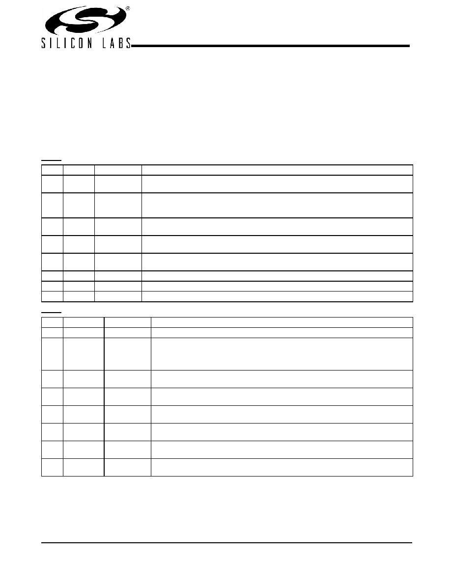
Byte 0: CPU Clock Register[2,3]
Bit
@Pup
Pin#
Description
7
0
Spread Spectrum Enable. 0 = Spread Off, 1 = Spread On
This is a Read and Write control bit.
6
0
CPU Clock Power-down Mode Select. 0 = Drive CPUT(0:2) to 4 or 6 IREF and drive
CPUC(0:2) LOW when PD# is asserted LOW. 1 = Tri-state all CPU outputs. This is only
applicable when PD# is LOW. It is not applicable to CPU_STP#.
5
0
35
3V66_1/VCH Frequency Select, 0 = 66M selected, 1 = 48M selected
This is a Read and Write control bit.
4
Pin 53
44,45,48,49,5
1,52
CPU_STP#. Reflects the current value of the external CPU_STP# (pin 53) This bit is
Read-only.
3
Pin 34
10,11,12,13,16
,17,18
Reflects the current value of the internal PCI_STP# function when read. Internally PCI_STP#
is a logical AND function of the internal SMBus register bit and the external PCI_STP# pin.
2
Pin 40
Frequency Select Bit 2. Reflects the value of SEL2 (pin 40). This bit is Read-only.
1
Pin 55
Frequency Select Bit 1. Reflects the value of SEL1 (pin 55). This bit is Read-only.
0
Pin 54
Frequency Select Bit 0. Reflects the value of SEL0 (pin 54). This bit is Read-only.
Byte 1: CPU Clock Register
Bit
@Pup
Pin#
Description
7
Pin 43
43
MULT0 (Pin 43) Value. This bit is Read-only.
6
0
53
CPUT/C(0:2) Output Functionality Control When CPU_STP# is Asserted. 0 = Drive
CPUT(0:2) to 4 or 6 IREF and drive CPUC(0:2) LOW when CPU_STP# asserted LOW.
1 = three-state all CPU outputs. This bit will override Byte0,Bit6 such that even if it is 0,
when PD# goes LOW the CPU outputs will be three-stated.
5
0
44,45
CPU2 Functionality Control When CPU_STP# is Asserted LOW. 1 = Free Running, 0 =
Stopped LOW with CPU_STP# asserted LOW. This is a Read and Write control bit.
4
0
48,49
CPU1 Functionality Control When CPU_STP# is Asserted LOW. 1 = Free Running, 0 =
Stopped LOW with CPU_STP# asserted LOW. This is a Read and Write control bit.
3
0
51,52
CPUT0 Functionality Control When CPU_STP# is Asserted LOW. 1 = Free Running, 0 =
Stopped LOW with CPU_STP# asserted LOW. This is a Read and Write control bit.
2
1
44,45
CPUT/C2 Output Control. 1 = enabled, 0 = disable HIGH and CPUC2 disables LOW. This
is a Read and Write control bit.
1
48,49
CPUT/C1 Output Control. 1 = enabled, 0 = disable HIGH and CPUC1 disables LOW. This
is a Read and Write control bit.
0
1
51,52
CPUT/C0 Output Control. 1 = enabled, 0 = disable HIGH and CPUC0 disables LOW. This
is a Read and Write control bit.
Notes:
2. PU = internal pull-up. PD = internal pull-down. T = tri-level logic input with valid logic voltages of LOW = < 0.8V, T = 1.0 – 1.8V and HIGH = > 2.0V.
3. The “Pin#” column lists the relevant pin number where applicable. The “@Pup” column gives the default state at power-up.
相关PDF资料 |
PDF描述 |
|---|---|
| VE-B32-MV-F2 | CONVERTER MOD DC/DC 15V 150W |
| VE-B32-MV-F1 | CONVERTER MOD DC/DC 15V 150W |
| VE-B31-MV-F4 | CONVERTER MOD DC/DC 12V 150W |
| ICS525RI-11LF | IC PECL CLK USER CONFIG 28-SSOP |
| IDTCSP2510DPGI8 | IC CLK DVR PLL ZDB 1:10 24TSSOP |
相关代理商/技术参数 |
参数描述 |
|---|---|
| CY28346ZXC-2 | 功能描述:时钟合成器/抖动清除器 NB Clk Intel Brkdale 830M & 845 chipsets RoHS:否 制造商:Skyworks Solutions, Inc. 输出端数量: 输出电平: 最大输出频率: 输入电平: 最大输入频率:6.1 GHz 电源电压-最大:3.3 V 电源电压-最小:2.7 V 封装 / 箱体:TSSOP-28 封装:Reel |
| CY28346ZXC-2T | 功能描述:时钟合成器/抖动清除器 NB Clk Intel Brkdale 830M & 845 chipsets RoHS:否 制造商:Skyworks Solutions, Inc. 输出端数量: 输出电平: 最大输出频率: 输入电平: 最大输入频率:6.1 GHz 电源电压-最大:3.3 V 电源电压-最小:2.7 V 封装 / 箱体:TSSOP-28 封装:Reel |
| CY28346ZXCT | 功能描述:时钟合成器/抖动清除器 NB Clk Intel Brkdale 830M & 845 chipsets RoHS:否 制造商:Skyworks Solutions, Inc. 输出端数量: 输出电平: 最大输出频率: 输入电平: 最大输入频率:6.1 GHz 电源电压-最大:3.3 V 电源电压-最小:2.7 V 封装 / 箱体:TSSOP-28 封装:Reel |
| CY28347 | 制造商:CYPRESS 制造商全称:Cypress Semiconductor 功能描述:Universal Single-chip Clock Solution for VIA P4M266/KM266 DDR Systems |
| CY28347OC | 制造商:CYPRESS 制造商全称:Cypress Semiconductor 功能描述:Universal Single-chip Clock Solution for VIA P4M266/KM266 DDR Systems |
发布紧急采购,3分钟左右您将得到回复。