- 您现在的位置:买卖IC网 > PDF目录9026 > CY28346ZXC (Silicon Laboratories Inc)IC CLOCK DIFF OUT CK408 56TSSOP PDF资料下载
参数资料
| 型号: | CY28346ZXC |
| 厂商: | Silicon Laboratories Inc |
| 文件页数: | 16/19页 |
| 文件大小: | 0K |
| 描述: | IC CLOCK DIFF OUT CK408 56TSSOP |
| 标准包装: | 35 |
| 类型: | * |
| PLL: | 是 |
| 输入: | 晶体 |
| 输出: | 时钟 |
| 电路数: | 1 |
| 比率 - 输入:输出: | 1:19 |
| 差分 - 输入:输出: | 无/是 |
| 频率 - 最大: | 200MHz |
| 除法器/乘法器: | 是/无 |
| 电源电压: | 3.135 V ~ 3.465 V |
| 工作温度: | 0°C ~ 70°C |
| 安装类型: | * |
| 封装/外壳: | * |
| 供应商设备封装: | * |
| 包装: | * |
| 其它名称: | SLCY28346ZXC |
CY28346
........................Document #: 38-07331 Rev. *C Page 6 of 19
Dial-a-Frequency Features
SMBus Dial-a-Frequency feature is available in this device via
Byte8 and Byte9.
P is a large-value PLL constant that depends on the frequency
selection achieved through the hardware selectors (S1, S0). P
value may be determined from Table 2.
Dial-a-dB Features
SMBus Dial-a-dB feature is available in this device via Byte8
and Byte9.
Spread Spectrum Clock Generation (SSCG)
Spread Spectrum is a modulation technique used to
minimizing EMI radiation generated by repetitive digital
signals. A clock presents the greatest EMI energy at the center
frequency it is generating. Spread Spectrum distributes this
energy over a specific and controlled frequency bandwidth
therefore causing the average energy at any one point in this
band to decrease in value. This technique is achieved by
modulating the clock away from its resting frequency by a
certain percentage (which also determines the amount of EMI
reduction). In this device, Spread Spectrum is enabled by
setting specific register bits in the SMBus control bytes.
Table 3 is a listing of the modes and percentages of Spread
Spectrum modulation that this device incorporates.
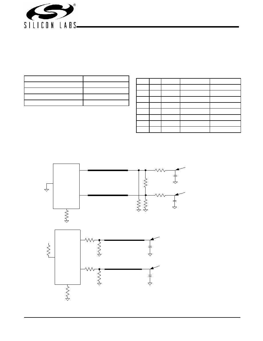
Test and Measurement Set-up
For Differential CPU Output Signals
The following diagram shows lumped test load configurations
for the differential Host Clock Outputs.
Table 2. P Value
S(1:0)
P
0 0
32005333
0 1
48008000
1 0
96016000
1 1
64010667
Table 3. Spread Spectrum
SS2
SS1
SS0
Spread Mode
Spread%
0
Down
+0.00, –0.25
0
1
Down
+0.00, –0.50
0
1
0
Down
+0.00, –0.75
0
1
Down
+0.00, –1.00
1
0
Center
+0.13, –0.13
1
0
1
Center
+0.25, –0.25
1
0
Center
+0.37, –0.37
1
Center
+0.50, –1.50
M eas urem en t P oint
2p F
CP U T
M U L T SEL
T
PCB
T
PCB
CP U C
M easurem ent P o int
2p F
Figure 1. 1.0V Test Load Termination
CPUT
MULTSEL
T
PCB
T
PCB
CPUC
Measurement Point
2pF
Measurement Point
2pF
VDD
Figure 2. 0.7V Test Load Termination
相关PDF资料 |
PDF描述 |
|---|---|
| VE-B32-MV-F2 | CONVERTER MOD DC/DC 15V 150W |
| VE-B32-MV-F1 | CONVERTER MOD DC/DC 15V 150W |
| VE-B31-MV-F4 | CONVERTER MOD DC/DC 12V 150W |
| ICS525RI-11LF | IC PECL CLK USER CONFIG 28-SSOP |
| IDTCSP2510DPGI8 | IC CLK DVR PLL ZDB 1:10 24TSSOP |
相关代理商/技术参数 |
参数描述 |
|---|---|
| CY28346ZXC-2 | 功能描述:时钟合成器/抖动清除器 NB Clk Intel Brkdale 830M & 845 chipsets RoHS:否 制造商:Skyworks Solutions, Inc. 输出端数量: 输出电平: 最大输出频率: 输入电平: 最大输入频率:6.1 GHz 电源电压-最大:3.3 V 电源电压-最小:2.7 V 封装 / 箱体:TSSOP-28 封装:Reel |
| CY28346ZXC-2T | 功能描述:时钟合成器/抖动清除器 NB Clk Intel Brkdale 830M & 845 chipsets RoHS:否 制造商:Skyworks Solutions, Inc. 输出端数量: 输出电平: 最大输出频率: 输入电平: 最大输入频率:6.1 GHz 电源电压-最大:3.3 V 电源电压-最小:2.7 V 封装 / 箱体:TSSOP-28 封装:Reel |
| CY28346ZXCT | 功能描述:时钟合成器/抖动清除器 NB Clk Intel Brkdale 830M & 845 chipsets RoHS:否 制造商:Skyworks Solutions, Inc. 输出端数量: 输出电平: 最大输出频率: 输入电平: 最大输入频率:6.1 GHz 电源电压-最大:3.3 V 电源电压-最小:2.7 V 封装 / 箱体:TSSOP-28 封装:Reel |
| CY28347 | 制造商:CYPRESS 制造商全称:Cypress Semiconductor 功能描述:Universal Single-chip Clock Solution for VIA P4M266/KM266 DDR Systems |
| CY28347OC | 制造商:CYPRESS 制造商全称:Cypress Semiconductor 功能描述:Universal Single-chip Clock Solution for VIA P4M266/KM266 DDR Systems |
发布紧急采购,3分钟左右您将得到回复。