- 您现在的位置:买卖IC网 > PDF目录9026 > CY28346ZXC (Silicon Laboratories Inc)IC CLOCK DIFF OUT CK408 56TSSOP PDF资料下载
参数资料
| 型号: | CY28346ZXC |
| 厂商: | Silicon Laboratories Inc |
| 文件页数: | 12/19页 |
| 文件大小: | 0K |
| 描述: | IC CLOCK DIFF OUT CK408 56TSSOP |
| 标准包装: | 35 |
| 类型: | * |
| PLL: | 是 |
| 输入: | 晶体 |
| 输出: | 时钟 |
| 电路数: | 1 |
| 比率 - 输入:输出: | 1:19 |
| 差分 - 输入:输出: | 无/是 |
| 频率 - 最大: | 200MHz |
| 除法器/乘法器: | 是/无 |
| 电源电压: | 3.135 V ~ 3.465 V |
| 工作温度: | 0°C ~ 70°C |
| 安装类型: | * |
| 封装/外壳: | * |
| 供应商设备封装: | * |
| 包装: | * |
| 其它名称: | SLCY28346ZXC |
CY28346
........................Document #: 38-07331 Rev. *C Page 2 of 19
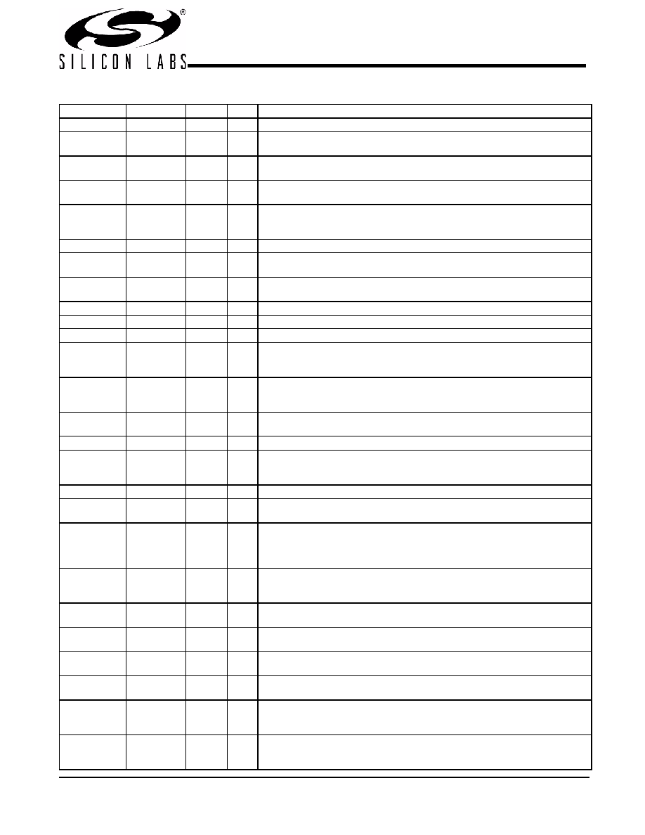
Pin Description
Pin
Name
PWR
I/O
Description
2XIN
I
Oscillator Buffer Input. Connect to a crystal or to an external clock.
3XOUT
VDD
O
Oscillator Buffer Output. Connect to a crystal. Do not connect when an external
clock is applied at XIN.
52, 51, 49, 48,
45, 44
CPUT(0:2),
CPUC(0:2)
VDD
O
Differential Host Output Clock Pairs. See Table 1 for frequency/functionality.
10, 11, 12, 13,
16, 17, 18
PCI(0:6)
VDDP
O
PCI Clock Outputs. Are synchronous to 66IN or 3V66 clock. See Table 1.
5, 6, 7
PCIF (0:2)
VDD
O
33MHz PCI Clocks.
2 copies of 66IN or 3V66 clocks that may be free running
(not stopped when PCI_STP# is asserted LOW) or may be stoppable depending
on the programming of SMBus register Byte3,Bits (3:5).
56
REF
VDD
O
Buffered Output Copy of the Device’s XIN Clock.
42
IREF
VDD
I
Current Reference Programming Input for CPU Buffers. A resistor is
connected between this pin and VSSIREF.
28
VTT_PG#
VDD
I
Qualifying Input that Latches S(0:2) and MULT0. When this input is at a logic
LOW, the S(0:2) and MULT0 are latched.
39
48MUSB
VDD48
O
Fixed 48 MHz USB Clock Outputs.
38
48MDOT
VDD48
O
Fixed 48 MHZ DOT Clock Outputs.
33
3V66_0
VDD
O
3.3V 66 MHz Fixed-frequency Clock.
35
3V66_1/VCH
VDD
O
3.3V Clock Selectable with SMBus Byte0,Bit5, When Byte5,Bit5. When Byte
0,Bit 5 is at a logic 1, then this pin is a 48M output clock. When Byte0,Bit5 is a
logic 0, this is a 66M output clock (default).
25
PD#
VDD
I
PU
Power-down Mode Pin. A logic LOW level causes the device to enter a
power-down state. All internal logic is turned off except for the SMBus logic. All
output buffers are stopped.
43
MULT0
I
PU
Programming Input Selection for CPU Clock Current Multiplier.
55, 54
S(0,1)
I
Frequency Select Inputs. See Table 1.
29
SDATA
I
Serial Data Input. Conforms to the SMBus specification of a Slave
Receive/Transmit device. It is an input when receiving data. It is an open drain
output when acknowledging or transmitting data.
30
SCLK
I
Serial Clock Input. Conforms to the SMBus specification.
40
S2
VDD
I
T
Frequency Select Input. See Table 1. This is a Tri-level input which is driven
HIGH, LOW or driven to a intermediate level.
34
PCI_STP#
VDD
I
PU
PCI Clock Disable Input. When asserted LOW, PCI (0:6) clocks are synchro-
nously disabled in a LOW state. This pin does not effect PCIF (0:2) clocks’
outputs if they are programmed to be PCIF clocks via the device’s SMBus
interface.
53
CPU_STP#
VDD
I
PU
CPU Clock Disable Input. When asserted LOW, CPUT (0:2) clocks are
synchronously disabled in a HIGH state and CPUC(0:2) clocks are synchro-
nously disabled in a LOW state.
24
66IN/3V66_5
VDD
I/O
Input Connection for 66CLK(0:2) Output Clock Buffers if S2 = 1, or output
clock for fixed 66-MHz clock if S2 = 0. See Table 1.
21, 22, 23
66B(0:2)/
3V66(2:4)
VDD
O
3.3V Clock Outputs. These clocks are buffered copies of the 66IN clock or fixed
at 66 MHz. See Table 1.
1, 8, 14, 19, 32,
37, 46, 50
VDD
PWR 3.3V Power Supply.
4, 9, 15, 20, 27,
31, 36, 47
VSS
PWR Common Ground.
41
VSSIREF
PWR Current Reference Programming Input for CPU Buffers. A resistor is
connected between this pin and IREF. This pin should also be returned to device
VSS.
26
VDDA
–PWR Analog Power Input. Used for phase-locked loops (PLLs) and internal analog
circuits. It is also specifically used to detect and determine when power is at an
acceptable level to enable the device to operate.
相关PDF资料 |
PDF描述 |
|---|---|
| VE-B32-MV-F2 | CONVERTER MOD DC/DC 15V 150W |
| VE-B32-MV-F1 | CONVERTER MOD DC/DC 15V 150W |
| VE-B31-MV-F4 | CONVERTER MOD DC/DC 12V 150W |
| ICS525RI-11LF | IC PECL CLK USER CONFIG 28-SSOP |
| IDTCSP2510DPGI8 | IC CLK DVR PLL ZDB 1:10 24TSSOP |
相关代理商/技术参数 |
参数描述 |
|---|---|
| CY28346ZXC-2 | 功能描述:时钟合成器/抖动清除器 NB Clk Intel Brkdale 830M & 845 chipsets RoHS:否 制造商:Skyworks Solutions, Inc. 输出端数量: 输出电平: 最大输出频率: 输入电平: 最大输入频率:6.1 GHz 电源电压-最大:3.3 V 电源电压-最小:2.7 V 封装 / 箱体:TSSOP-28 封装:Reel |
| CY28346ZXC-2T | 功能描述:时钟合成器/抖动清除器 NB Clk Intel Brkdale 830M & 845 chipsets RoHS:否 制造商:Skyworks Solutions, Inc. 输出端数量: 输出电平: 最大输出频率: 输入电平: 最大输入频率:6.1 GHz 电源电压-最大:3.3 V 电源电压-最小:2.7 V 封装 / 箱体:TSSOP-28 封装:Reel |
| CY28346ZXCT | 功能描述:时钟合成器/抖动清除器 NB Clk Intel Brkdale 830M & 845 chipsets RoHS:否 制造商:Skyworks Solutions, Inc. 输出端数量: 输出电平: 最大输出频率: 输入电平: 最大输入频率:6.1 GHz 电源电压-最大:3.3 V 电源电压-最小:2.7 V 封装 / 箱体:TSSOP-28 封装:Reel |
| CY28347 | 制造商:CYPRESS 制造商全称:Cypress Semiconductor 功能描述:Universal Single-chip Clock Solution for VIA P4M266/KM266 DDR Systems |
| CY28347OC | 制造商:CYPRESS 制造商全称:Cypress Semiconductor 功能描述:Universal Single-chip Clock Solution for VIA P4M266/KM266 DDR Systems |
发布紧急采购,3分钟左右您将得到回复。