- 您现在的位置:买卖IC网 > PDF目录9586 > CY28447LFXCT (Silicon Laboratories Inc)IC CLOCK CALISTOGA CK410M 72QFN PDF资料下载
参数资料
| 型号: | CY28447LFXCT |
| 厂商: | Silicon Laboratories Inc |
| 文件页数: | 2/22页 |
| 文件大小: | 0K |
| 描述: | IC CLOCK CALISTOGA CK410M 72QFN |
| 标准包装: | 2,000 |
| 类型: | 时钟/频率发生器 |
| PLL: | 是 |
| 主要目的: | Intel CPU 服务器 |
| 输入: | LVTTL,晶体 |
| 输出: | HCSL,LVCMOS |
| 电路数: | 1 |
| 比率 - 输入:输出: | 3:21 |
| 差分 - 输入:输出: | 无/是 |
| 频率 - 最大: | 200MHz |
| 电源电压: | 3.135 V ~ 3.465 V |
| 工作温度: | 0°C ~ 85°C |
| 安装类型: | 表面贴装 |
| 封装/外壳: | 72-VFQFN 裸露焊盘 |
| 供应商设备封装: | 72-QFN(10x10) |
| 包装: | 带卷 (TR) |
CY28447
...................... Document #: 38-07724 Rev *C Page 10 of 22
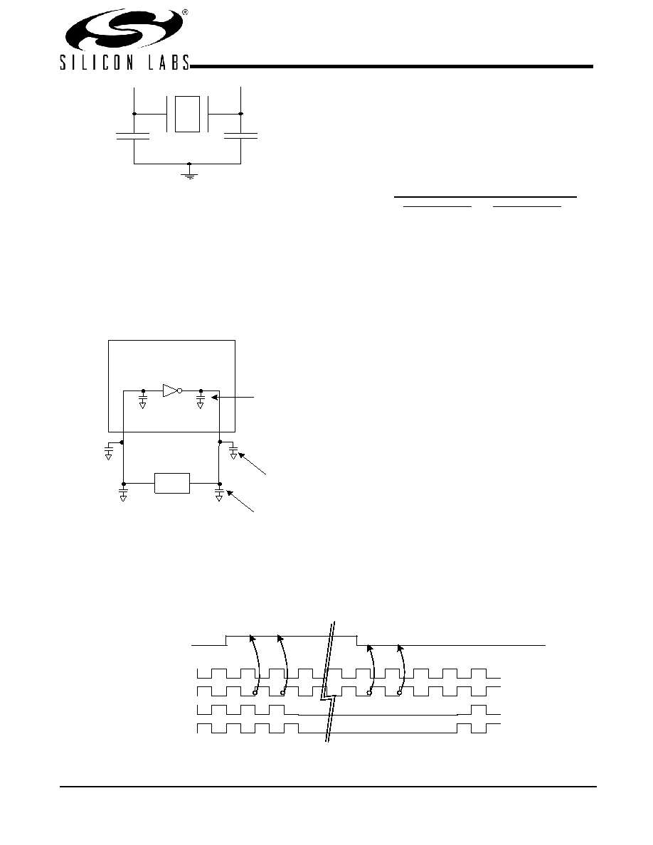
Calculating Load Capacitors
In addition to the standard external trim capacitors, trace
capacitance and pin capacitance must also be considered to
correctly calculate crystal loading. As mentioned previously,
the capacitance on each side of the crystal is in series with the
crystal. This means the total capacitance on each side of the
crystal must be twice the specified crystal load capacitance
(CL). While the capacitance on each side of the crystal is in
series with the crystal, trim capacitors (Ce1,Ce2) should be
calculated to provide equal capacitive loading on both sides.
As mentioned previously, the capacitance on each side of the
crystal is in series with the crystal. This means the total capac-
itance on each side of the crystal must be twice the specified
load capacitance (CL). While the capacitance on each side of
the crystal is in series with the crystal, trim capacitors
(Ce1,Ce2) should be calculated to provide equal capacitance
loading on both sides.
Use the following formulas to calculate the trim capacitor
values for Ce1 and Ce2.
CL....................................................Crystal load capacitance
CLe......................................... Actual loading seen by crystal
using standard value trim capacitors
Ce..................................................... External trim capacitors
Cs .............................................. Stray capacitance (terraced)
Ci ...........................................................Internal capacitance
(lead frame, bond wires etc.)
CLK_REQ# Description
The CLKREQ# signals are active LOW inputs used for clean
enabling and disabling selected SRC outputs. The outputs
controlled by CLKREQ# are determined by the settings in
register byte 8. The CLKREQ# signal is a de-bounced signal
in that it’s state must remain unchanged during two consec-
utive rising edges of SRCC to be recognized as a valid
assertion or deassertion. (The assertion and deassertion of
this signal is absolutely asynchronous.)
CLK_REQ[1:9]# Assertion (CLKREQ# -> LOW)
All differential outputs that were stopped are to resume normal
operation in a glitch-free manner. The maximum latency from
the assertion to active outputs is between 2 and 6 SRC clock
periods (2 clocks are shown) with all SRC outputs resuming
simultaneously. All stopped SRC outputs must be driven HIGH
within 10 ns of CLKREQ# deassertion to a voltage greater than
200 mV.
CLK_REQ[1:9]# Deassertion (CLKREQ# -> HIGH)
The impact of deasserting the CLKREQ# pins is that all SRC
outputs that are set in the control registers to stoppable via
deassertion of CLKREQ# are to be stopped after their next
transition. The final state of all stopped DIF signals is LOW,
both SRCT clock and SRCC clock outputs will not be driven.
Figure 1. Crystal Capacitive Clarification
XTAL
Ce2
Ce1
Cs1
Cs2
X1
X2
Ci1
Ci2
Clock Chip
Trace
2.8 pF
Trim
33 pF
Pin
3 to 6p
Figure 2. Crystal Loading Example
Load Capacitance (each side)
Total Capacitance (as seen by the crystal)
Ce = 2 * CL – (Cs + Ci)
Ce1 + Cs1 + Ci1
1
+
Ce2 + Cs2 + Ci2
1
()
1
=
CLe
Figure 3. CLK_REQ#[1:9] Deassertion/Assertion Waveform
SRCT(stoppable)
SRCC(free running)
SRCT(free running)
CLKREQ#X
相关PDF资料 |
PDF描述 |
|---|---|
| VE-B3H-MY-S | CONVERTER MOD DC/DC 52V 50W |
| VE-B53-IU | CONVERTER MOD DC/DC 24V 200W |
| ICS932S200BFLF | IC FREQ TIMING GENERATOR 56-SSOP |
| VE-B31-MY-S | CONVERTER MOD DC/DC 12V 50W |
| VE-B4J-IU | CONVERTER MOD DC/DC 36V 200W |
相关代理商/技术参数 |
参数描述 |
|---|---|
| CY28506OC | 制造商:Rochester Electronics LLC 功能描述:FTG FOR MOTHERBOARDS - Bulk |
| CY28506OCT | 制造商:Rochester Electronics LLC 功能描述:CLOC - Tape and Reel |
| CY28507ZC-3 | 功能描述:时钟缓冲器 PacketClockClk RoHS:否 制造商:Texas Instruments 输出端数量:5 最大输入频率:40 MHz 传播延迟(最大值): 电源电压-最大:3.45 V 电源电压-最小:2.375 V 最大功率耗散: 最大工作温度:+ 85 C 最小工作温度:- 40 C 封装 / 箱体:LLP-24 封装:Reel |
| CY28508OCT | 制造商:Cypress Semiconductor 功能描述: |
| CY28508OXC | 功能描述:时钟发生器及支持产品 Power PC RoHS:否 制造商:Silicon Labs 类型:Clock Generators 最大输入频率:14.318 MHz 最大输出频率:166 MHz 输出端数量:16 占空比 - 最大:55 % 工作电源电压:3.3 V 工作电源电流:1 mA 最大工作温度:+ 85 C 安装风格:SMD/SMT 封装 / 箱体:QFN-56 |
发布紧急采购,3分钟左右您将得到回复。