- 您现在的位置:买卖IC网 > PDF目录9586 > CY28447LFXCT (Silicon Laboratories Inc)IC CLOCK CALISTOGA CK410M 72QFN PDF资料下载
参数资料
| 型号: | CY28447LFXCT |
| 厂商: | Silicon Laboratories Inc |
| 文件页数: | 3/22页 |
| 文件大小: | 0K |
| 描述: | IC CLOCK CALISTOGA CK410M 72QFN |
| 标准包装: | 2,000 |
| 类型: | 时钟/频率发生器 |
| PLL: | 是 |
| 主要目的: | Intel CPU 服务器 |
| 输入: | LVTTL,晶体 |
| 输出: | HCSL,LVCMOS |
| 电路数: | 1 |
| 比率 - 输入:输出: | 3:21 |
| 差分 - 输入:输出: | 无/是 |
| 频率 - 最大: | 200MHz |
| 电源电压: | 3.135 V ~ 3.465 V |
| 工作温度: | 0°C ~ 85°C |
| 安装类型: | 表面贴装 |
| 封装/外壳: | 72-VFQFN 裸露焊盘 |
| 供应商设备封装: | 72-QFN(10x10) |
| 包装: | 带卷 (TR) |
CY28447
.......................Document #: 38-07724 Rev *C Page 11 of 22
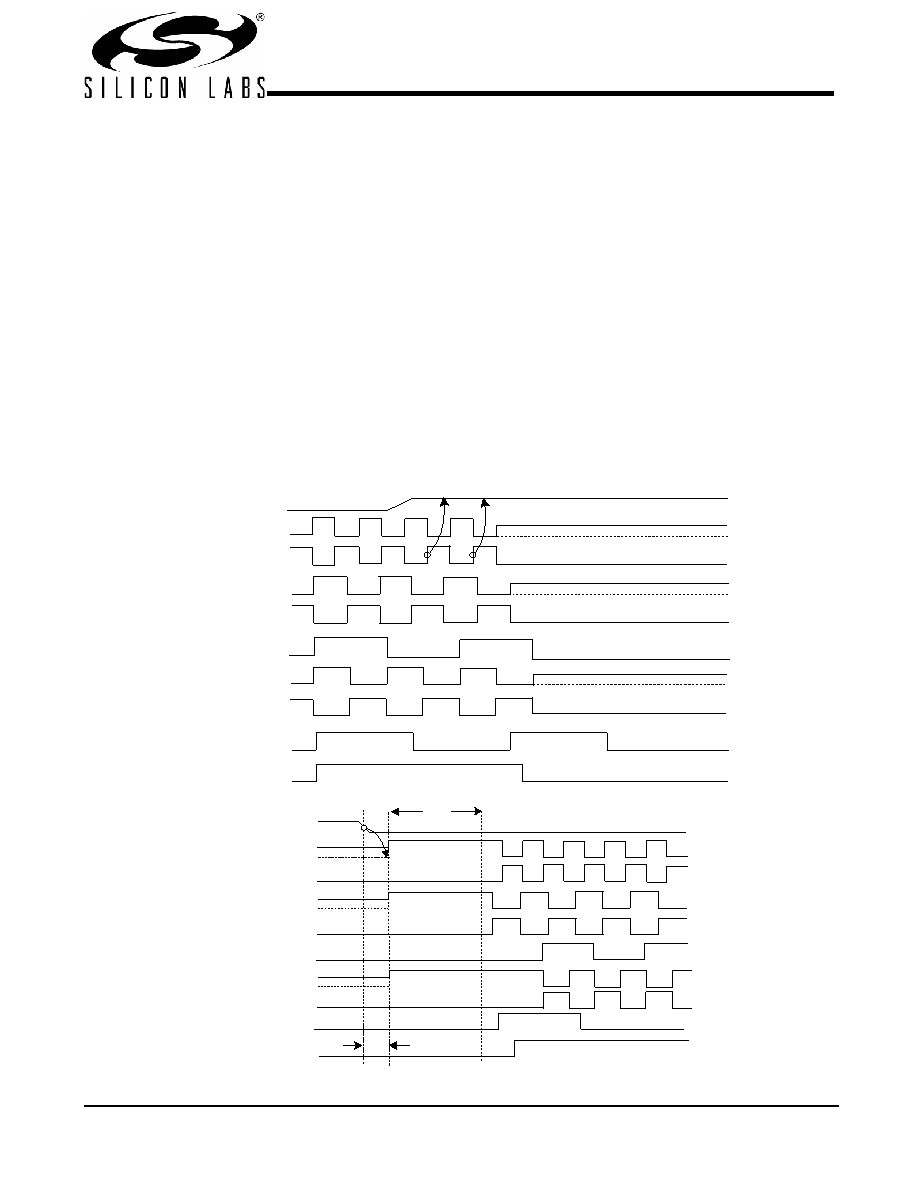
PD (Power-down) Clarification
The VTT_PWRGD# /PD pin is a dual-function pin. During
initial power-up, the pin functions as VTT_PWRGD#. Once
VTT_PWRGD# has been sampled LOW by the clock chip, the
pin assumes PD functionality. The PD pin is an asynchronous
active HIGH input used to shut off all clocks cleanly prior to
shutting off power to the device. This signal is synchronized
internal to the device prior to powering down the clock synthe-
sizer. PD is also an asynchronous input for powering up the
system. When PD is asserted HIGH, all clocks need to be
driven to a LOW value and held prior to turning off the VCOs
and the crystal oscillator.
PD (Power-down) Assertion
When PD is sampled HIGH by two consecutive rising edges
of CPUC, all single-ended outputs will be held LOW on their
next HIGH-to-LOW transition and differential clocks must be
held HIGH or tri-stated (depending on the state of the control
register drive mode bit) on the next diff clock# HIGH-to-LOW
transition within 4 clock periods. When the SMBus PD drive
mode bit corresponding to the differential (CPU, SRC, and
DOT) clock output of interest is programmed to ‘0’, the clock
outputs are held with “Diff clock” pin driven HIGH at 2 x Iref,
and “Diff clock#” tri-state. If the control register PD drive mode
bit corresponding to the output of interest is programmed to
“1”, then both the “Diff clock” and the “Diff clock#” are tri-state.
Note that Figure 4 shows CPUT = 133 MHz and PD drive
mode = ‘1’ for all differential outputs. This diagram and
description is applicable to valid CPU frequencies 100, 133,
166, and 200 MHz. In the event that PD mode is desired as
the initial power-on state, PD must be asserted HIGH in less
than 10
s after asserting Vtt_PwrGd#. It should be noted that
96_100_SSC will follow the DOT waveform is selected for
96 MHz and the SRC waveform when in 100-MHz mode.
PD Deassertion
The power-up latency is less than 1.8 ms. This is the time from
the deassertion of the PD pin or the ramping of the power
supply until the time that stable clocks are output from the
clock chip. All differential outputs stopped in a three-state
condition resulting from power down will be driven high in less
than 300
s of PD deassertion to a voltage greater than
200 mV. After the clock chip’s internal PLL is powered up and
locked, all outputs will be enabled within a few clock cycles of
each other. Figure 5 is an example showing the relationship of
clocks coming up. It should be noted that 96_100_SSC will
follow the DOT waveform is selected for 96 MHz and the SRC
waveform when in 100-MHz mode.
Figure 4. Power-down Assertion Timing Waveform
PD
USB, 48MHz
DOT96T
DOT96C
SRCT 100MHz
SRCC 100MHz
CPUT, 133MHz
PCI, 33 MHz
REF
CPUC, 133MHz
Figure 5. Power-down Deassertion Timing Waveform
DOT96C
PD
CPUC, 133MHz
CPUT, 133MHz
SRCC 100MHz
USB, 48MHz
DOT96T
SRCT 100MHz
Tstable
<1.8 ms
PCI, 33MHz
REF
Tdrive_PWRDN#
<300
s, >200 mV
相关PDF资料 |
PDF描述 |
|---|---|
| VE-B3H-MY-S | CONVERTER MOD DC/DC 52V 50W |
| VE-B53-IU | CONVERTER MOD DC/DC 24V 200W |
| ICS932S200BFLF | IC FREQ TIMING GENERATOR 56-SSOP |
| VE-B31-MY-S | CONVERTER MOD DC/DC 12V 50W |
| VE-B4J-IU | CONVERTER MOD DC/DC 36V 200W |
相关代理商/技术参数 |
参数描述 |
|---|---|
| CY28506OC | 制造商:Rochester Electronics LLC 功能描述:FTG FOR MOTHERBOARDS - Bulk |
| CY28506OCT | 制造商:Rochester Electronics LLC 功能描述:CLOC - Tape and Reel |
| CY28507ZC-3 | 功能描述:时钟缓冲器 PacketClockClk RoHS:否 制造商:Texas Instruments 输出端数量:5 最大输入频率:40 MHz 传播延迟(最大值): 电源电压-最大:3.45 V 电源电压-最小:2.375 V 最大功率耗散: 最大工作温度:+ 85 C 最小工作温度:- 40 C 封装 / 箱体:LLP-24 封装:Reel |
| CY28508OCT | 制造商:Cypress Semiconductor 功能描述: |
| CY28508OXC | 功能描述:时钟发生器及支持产品 Power PC RoHS:否 制造商:Silicon Labs 类型:Clock Generators 最大输入频率:14.318 MHz 最大输出频率:166 MHz 输出端数量:16 占空比 - 最大:55 % 工作电源电压:3.3 V 工作电源电流:1 mA 最大工作温度:+ 85 C 安装风格:SMD/SMT 封装 / 箱体:QFN-56 |
发布紧急采购,3分钟左右您将得到回复。