- 您现在的位置:买卖IC网 > PDF目录295354 > CY7C09099V-6AXC (CYPRESS SEMICONDUCTOR CORP) 3.3V 32K/64K/128K x 8/9 Synchronous Dual-Port Static RAM PDF资料下载
参数资料
| 型号: | CY7C09099V-6AXC |
| 厂商: | CYPRESS SEMICONDUCTOR CORP |
| 元件分类: | SRAM |
| 英文描述: | 3.3V 32K/64K/128K x 8/9 Synchronous Dual-Port Static RAM |
| 中文描述: | 128K X 8 DUAL-PORT SRAM, 15 ns, PQFP100 |
| 封装: | ROHS COMPLIANT, PLASTIC, MS-026, TQFP-100 |
| 文件页数: | 12/20页 |
| 文件大小: | 599K |
| 代理商: | CY7C09099V-6AXC |
CY7C09079V/89V/99V
CY7C09179V/89V/99V
Document #: 38-06043 Rev. *E
Page 2 of 20
Functional Description
The CY7C09079V/89V/99V and CY7C09179V/89V/99V are
high speed synchronous CMOS 32K, 64K, and 128K x 8/9
dual-port static RAMs. Two ports are provided, permitting
independent, simultaneous access for reads and writes to any
location in memory.[4] Registers on control, address, and data
lines enable minimal setup and hold times. In pipelined output
mode, data is registered for decreased cycle time. Clock to data
used to bypass the pipelined output register to eliminate access
latency. In flow-through mode, data is available tCD1 = 18 ns after
the address is clocked into the device. Pipelined output or
flow-through mode is selected via the FT/Pipe pin.
Each port contains a burst counter on the input address register.
The internal write pulse width is independent of the
LOW-to-HIGH transition of the clock signal. The internal write
pulse is self-timed to enable the shortest possible cycle times.
A HIGH on CE0 or LOW on CE1 for one clock cycle powers down
the internal circuitry to reduce the static power consumption. The
use of multiple Chip Enables enables easier banking of multiple
chips for depth expansion configurations. In the pipelined mode,
one cycle is required with CE0 LOW and CE1 HIGH to reactivate
the outputs.
Counter enable inputs are provided to stall the operation of the
address input and use the internal address generated by the
internal counter for fast interleaved memory applications. A
port’s burst counter is loaded with the port’s Address Strobe
(ADS). When the port’s Count Enable (CNTEN) is asserted, the
address counter increments on each LOW-to-HIGH transition of
that port’s clock signal. This reads/writes one word from/into
each successive address location until CNTEN is deasserted.
The counter can address the entire memory array and loops
back to the start. Counter Reset (CNTRST) is used to reset the
burst counter.
All parts are available in 100-pin Thin Quad Plastic Flatpack
(TQFP) packages.
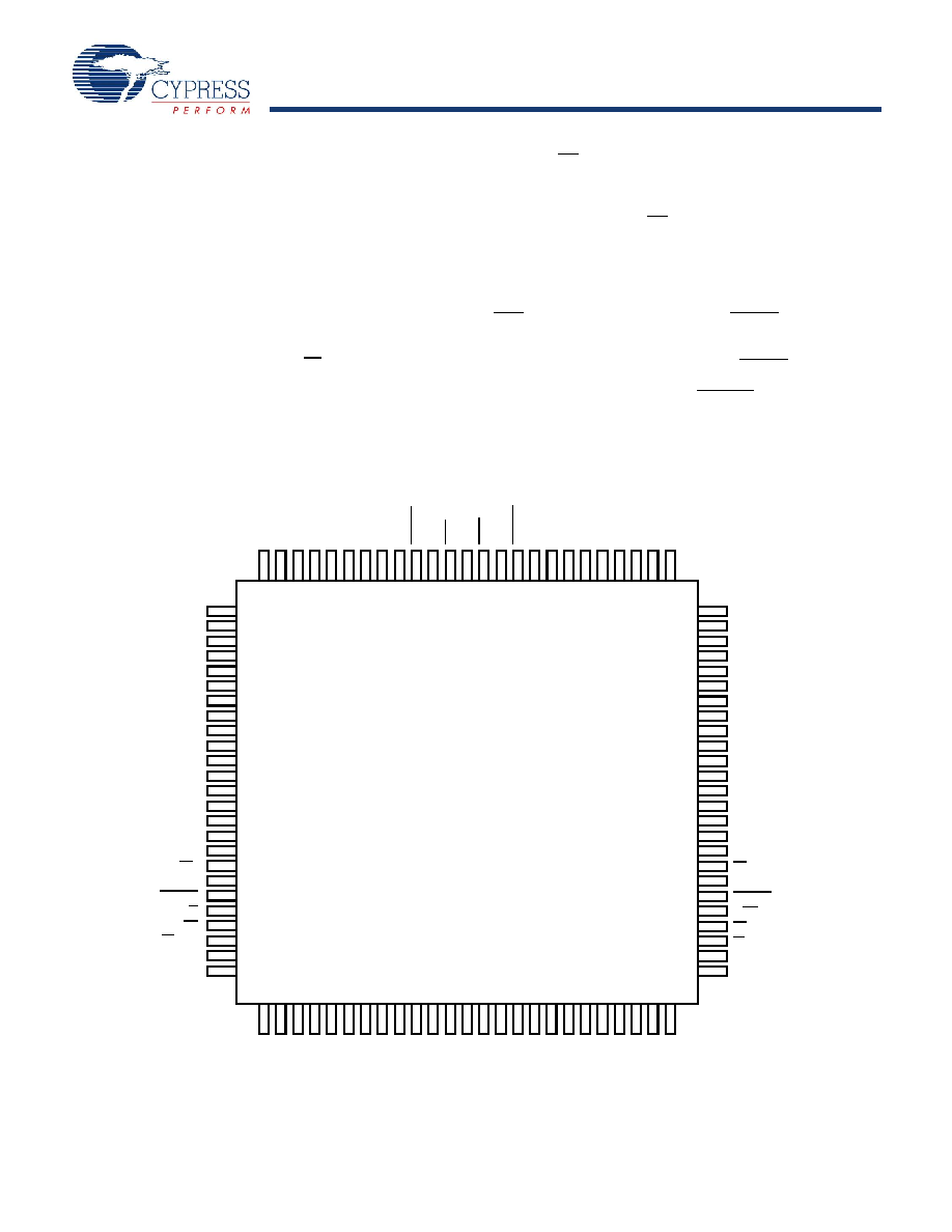
Pin Configurations
Figure 1. 100-Pin TQFP (Top View) - CY7C09099V (128K x 8), CY7C09089V (64K x 8),CY7C09079V (32K x 8)
Notes
4. When writing simultaneously to the same location, the final value cannot be guaranteed.
5. This pin is NC for CY7C09079V.
6. This pin is NC for CY7C09079V and CY7C09089V.
7. For CY7C09079V and CY7C09089V, pin #23 connected to VCC is pin compatible with an IDT 5V x8 pipelined device; connecting pin #23 and #53 to GND is pin
compatible with an IDT 5V x16 flow-through device.
1
3
2
92 91 90
84
85
87 86
88
89
83 82 81
76
78 77
79
80
93
94
95
96
97
98
99
100
59
60
61
67
66
64
65
63
62
68
69
70
75
73
74
72
71
NC
A7R
A8R
A9R
A10R
A15R
A12R
A14R
GND
NC
CE0R
A13R
A11R
NC
CE1R
CNTRSTR
R/WR
OER
FT/PIPER
GND
NC
A16R
58
57
56
55
54
53
52
51
NC
A7L
A8L
A9L
A10L
A15L
A12L
A14L
VCC
NC
CE0L
A13L
A11L
NC
CE1L
CNTRSTL
R/WL
OEL
FT/PIPEL
NC
A16L
17
16
15
9
10
12
11
13
14
8
7
6
4
5
18
19
20
21
22
23
24
25
NC
A6L
A5L
A4L
A3L
CL
K
L
A1L
CN
TENL
GND
AD
SR
A0R
A1R
A0L
A2L
CL
K
R
CN
TENR
A2R
A3R
A4R
A5R
A6R
NC
AD
SL
34 35 36
42
41
39 40
38
37
43 44 45
50
48 49
47
46
NC
I/O7R
I/O6R
I/O5R
I/01R
I/O3R
I/O2R
GN
D
VC
C
GN
D
I/O2
L
VC
C
I/O4R
I/O0
L
I/O1
L
I/O3
L
I/O4
L
I/O5
L
I/O6
L
I/O7
L
NC
GN
D
I/O0R
33
32
31
30
29
28
27
26
[5]
相关PDF资料 |
PDF描述 |
|---|---|
| CY7C09099V-7AI | 3.3V 32K/64K/128K x 8/9 Synchronous Dual-Port Static RAM |
| CY7C09099V-12AXC | 3.3V 32K/64K/128K x 8/9 Synchronous Dual-Port Static RAM |
| CY7C09099V-7AXI | 3.3V 32K/64K/128K x 8/9 Synchronous Dual-Port Static RAM |
| CY7C09179V-12AXC | 3.3V 32K/64K/128K x 8/9 Synchronous Dual-Port Static RAM |
| CY7C09179V-6AXC | 3.3V 32K/64K/128K x 8/9 Synchronous Dual-Port Static RAM |
相关代理商/技术参数 |
参数描述 |
|---|---|
| CY7C09099V-7AI | 制造商:Cypress Semiconductor 功能描述:SRAM SYNC DUAL 3.3V 1MBIT 128KX8 18NS/7.5NS 100TQFP - Bulk |
| CY7C09099V-7AXI | 功能描述:静态随机存取存储器 3.3V 128Kx8 IND Sync Dual Port 静态随机存取存储器 RoHS:否 制造商:Cypress Semiconductor 存储容量:16 Mbit 组织:1 M x 16 访问时间:55 ns 电源电压-最大:3.6 V 电源电压-最小:2.2 V 最大工作电流:22 uA 最大工作温度:+ 85 C 最小工作温度:- 40 C 安装风格:SMD/SMT 封装 / 箱体:TSOP-48 封装:Tray |
| CY7C09099V-9AC | 制造商:Cypress Semiconductor 功能描述:SRAM Chip Sync Dual 3.3V 1M-Bit 128K x 8 20ns/9ns 100-Pin TQFP |
| CY7C09099V-9AI | 制造商:Cypress Semiconductor 功能描述:SRAM Chip Sync Dual 3.3V 1M-Bit 128K x 8 20ns/9ns 100-Pin TQFP |
| CY7C09159AV-12AC | 功能描述:IC SRAM 72KBIT 12NS 100LQFP RoHS:否 类别:集成电路 (IC) >> 存储器 系列:- 标准包装:72 系列:- 格式 - 存储器:RAM 存储器类型:SRAM - 同步 存储容量:9M(256K x 36) 速度:75ns 接口:并联 电源电压:3.135 V ~ 3.465 V 工作温度:-40°C ~ 85°C 封装/外壳:100-LQFP 供应商设备封装:100-TQFP(14x14) 包装:托盘 其它名称:71V67703S75PFGI |
发布紧急采购,3分钟左右您将得到回复。