- 您现在的位置:买卖IC网 > PDF目录295373 > CY7C1069AV33-10BAC (CYPRESS SEMICONDUCTOR CORP) 2M x 8 Static RAM PDF资料下载
参数资料
| 型号: | CY7C1069AV33-10BAC |
| 厂商: | CYPRESS SEMICONDUCTOR CORP |
| 元件分类: | SRAM |
| 英文描述: | 2M x 8 Static RAM |
| 中文描述: | 2M X 8 STANDARD SRAM, 10 ns, PBGA60 |
| 封装: | 8 X 20 MM, 1.20 MM HEIGHT, FBGA-60 |
| 文件页数: | 8/12页 |
| 文件大小: | 460K |
| 代理商: | CY7C1069AV33-10BAC |
CY7C1069AV33
Document #: 38-05255 Rev. *G
Page 5
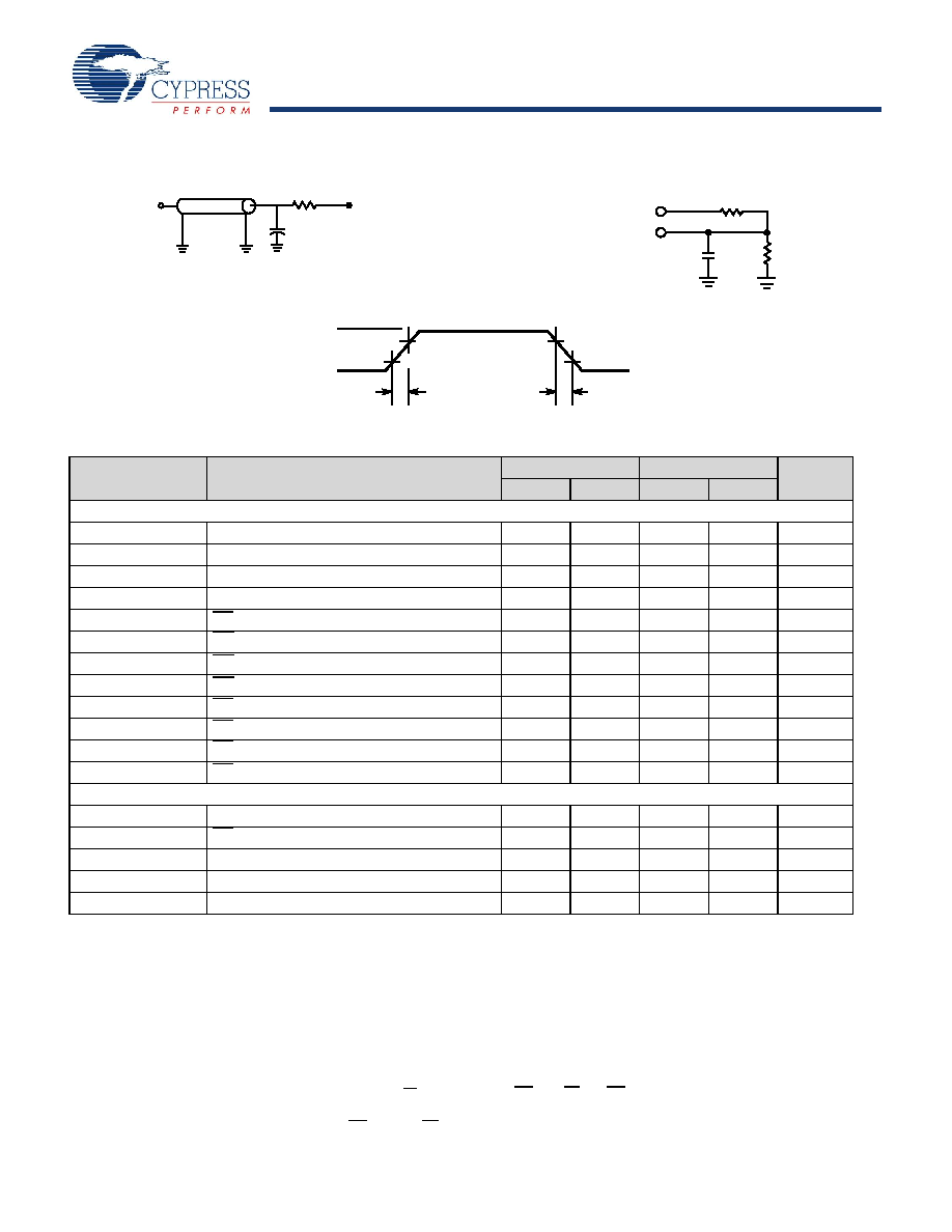
Figure 3. AC Test Loads and Waveforms[5]
Notes
5. Valid SRAM operation does not occur until the power supplies have reached the minimum operating VDD (3.0V). As soon as 1ms (Tpower) after reaching the
minimum operating VDD, normal SRAM operation can begin including reduction in VDD to the data retention (VCCDR, 2.0V) voltage.
6. Valid SRAM operation does not occur until the power supplies have reached the minimum operating VDD (3.0V). As soon as 1ms (Tpower) after reaching the
minimum operating VDD, normal SRAM operation can begin including reduction in VDD to the data retention (VCCDR, 2.0V) voltage.
7. Test conditions assume signal transition time of 3 ns or less, timing reference levels of 1.5V, input pulse levels of 0 to 3.0V, and output loading of the specified
IOL/IOH and transmission line loads. Test conditions for the Read cycle use output loading shown in part a) of the AC test loads, unless specified otherwise.
8. This part has a voltage regulator which steps down the voltage from 3V to 2V internally. tpower time has to be provided initially before a Read/Write operation
is started.
9. tHZOE, tHZCE, tHZWE and tLZOE, tLZCE, and tLZWE are specified with a load capacitance of 5 pF as in (b) of AC Test Loads. Transition is measured ±200 mV
from steady-state voltage.
10. These parameters are guaranteed by design and are not tested.
11. The internal Write time of the memory is defined by the overlap of CE1 LOW/CE2 HIGH, and WE LOW. CE1 and WE must be LOW along with CE2 HIGH to initiate
a Write, and the transition of any of these signals can terminate the Write. The input data setup and hold timing should be referenced to the leading edge of
the signal that terminates the Write.
12. The minimum Write cycle time for Write Cycle No. 3 (WE controlled, OE LOW) is the sum of tHZWE and tSD.
90%
10%
3.3V
GND
90%
10%
All input pulses
3.3V
OUTPUT
5 pF*
*Including
jig and
scope
(a)
(b)
R1 317
Ω
R2
351
Ω
Rise time > 1V/ns
Fall time: > 1V/ns
(c)
OUTPUT
50
Ω
Z0= 50Ω
VTH = 1.5V
30 pF* *Capacitive Load consists of all
components of the test environment
AC Switching Characteristics Over the Operating Range [7]
Parameter
Description
–10
–12
Unit
Min
Max
Min
Max
Read Cycle
tpower
11
ms
tRC
Read Cycle Time
10
12
ns
tAA
Address to Data Valid
10
12
ns
tOHA
Data Hold from Address Change
3
ns
tACE
CE1 LOW/CE2 HIGH to Data Valid
10
12
ns
tDOE
OE LOW to Data Valid
5
6
ns
tLZOE
OE LOW to Low-Z[9]
11
ns
tHZOE
OE HIGH to High-Z[9]
56
ns
tLZCE
CE1 LOW/CE2 HIGH to Low-Z
33
ns
tHZCE
56
ns
tPU
00
ns
tPD
CE1 HIGH/CE2 LOW to Power Down
10
12
ns
Write Cycle[10, 11]
tWC
Write Cycle Time
10
12
ns
tSCE
CE1 LOW/CE2 HIGH to Write End
7
8
ns
tAW
Address Setup to Write End
7
8
ns
tHA
Address Hold from Write End
0
ns
tSA
Address Setup to Write Start
0
ns
相关PDF资料 |
PDF描述 |
|---|---|
| CY7C1069AV33 | 2M x 8 Static RAM |
| CY7C109BL-15VC | 128K x 8 Static RAM |
| CY7C109BL-15VI | 128K x 8 Static RAM |
| CY7C109BL-15ZC | 128K x 8 Static RAM |
| CY7C1157V18-333BZC | 18-Mbit DDR-II+ SRAM 2-Word Burst Architecture (2.0 Cycle Read Latency) |
相关代理商/技术参数 |
参数描述 |
|---|---|
| CY7C1069AV33-10BAI | 制造商:Cypress Semiconductor 功能描述: |
| CY7C1069AV33-10ZC | 制造商:Cypress Semiconductor 功能描述: 制造商:Rochester Electronics LLC 功能描述: |
| CY7C1069AV33-10ZXC | 功能描述:静态随机存取存储器 2M x 8 CPG COM Fast Async 静态随机存取存储器 RoHS:否 制造商:Cypress Semiconductor 存储容量:16 Mbit 组织:1 M x 16 访问时间:55 ns 电源电压-最大:3.6 V 电源电压-最小:2.2 V 最大工作电流:22 uA 最大工作温度:+ 85 C 最小工作温度:- 40 C 安装风格:SMD/SMT 封装 / 箱体:TSOP-48 封装:Tray |
| CY7C1069AV33-10ZXCT | 功能描述:静态随机存取存储器 2M x 8 CPG COM Fast Async 静态随机存取存储器 RoHS:否 制造商:Cypress Semiconductor 存储容量:16 Mbit 组织:1 M x 16 访问时间:55 ns 电源电压-最大:3.6 V 电源电压-最小:2.2 V 最大工作电流:22 uA 最大工作温度:+ 85 C 最小工作温度:- 40 C 安装风格:SMD/SMT 封装 / 箱体:TSOP-48 封装:Tray |
| CY7C1069AV33-10ZXI | 功能描述:静态随机存取存储器 2M x 8 CPG IND Fast Async 静态随机存取存储器 RoHS:否 制造商:Cypress Semiconductor 存储容量:16 Mbit 组织:1 M x 16 访问时间:55 ns 电源电压-最大:3.6 V 电源电压-最小:2.2 V 最大工作电流:22 uA 最大工作温度:+ 85 C 最小工作温度:- 40 C 安装风格:SMD/SMT 封装 / 箱体:TSOP-48 封装:Tray |
发布紧急采购,3分钟左右您将得到回复。