参数资料
| 型号: | DAC8412FPZ |
| 厂商: | Analog Devices Inc |
| 文件页数: | 8/20页 |
| 文件大小: | 0K |
| 描述: | IC DAC 12BIT QUAD W/READBK 28DIP |
| 产品培训模块: | Data Converter Fundamentals DAC Architectures |
| 产品变化通告: | DAC8412/3 Redesign and Fab Process Change 01/Oct/2009 |
| 标准包装: | 13 |
| 设置时间: | 6µs |
| 位数: | 12 |
| 数据接口: | 并联 |
| 转换器数目: | 4 |
| 电压电源: | 单电源 |
| 功率耗散(最大): | 330mW |
| 工作温度: | -40°C ~ 85°C |
| 安装类型: | 通孔 |
| 封装/外壳: | 28-DIP(0.600",15.24mm) |
| 供应商设备封装: | 28-PDIP |
| 包装: | 管件 |
| 输出数目和类型: | 4 电压,单极;4 电压,双极 |
| 采样率(每秒): | 167k |
DAC8412/DAC8413
Data Sheet
Rev. G | Page 16 of 20
WRDB0
WRDB1
WRDB2
WRDB3
WRDB4
WRDB5
WRDB6
WRDB7
WRDB8
WRDB9
WRDB10
RDDACB
RDDACA
WRDACA
WRDACB
RDDACC
WRDACC
RDDACD
WRDACD
READBACKDATAIN_DB10
READOUT
READOUTBAR
READBACKDATAIN_DB11
A1
A0
DGND
R/W
DB11..DB0
VLOGIC
CS
DAC A
DAC B
DAC C
DAC D
WRDB11
INPUT
REGISTER
OUTPUT
REGISTER
VREFL
VOUTD
VOUTC
VOUTA
VOUTB
RESET
LDAC
VREFH
VDD VSS
READBACK
DATAOUT_DB11
00
27
4-
0
39
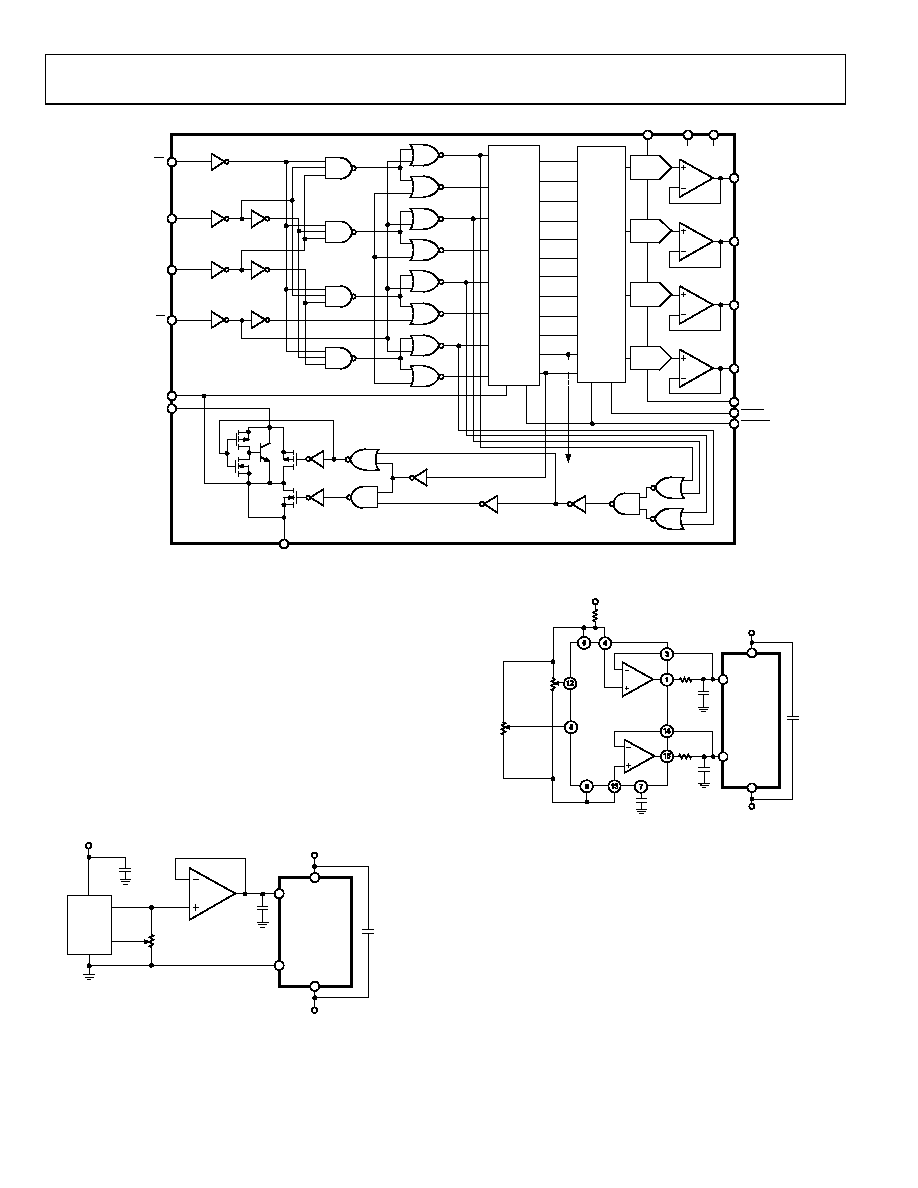
Figure 38. Simplified I/O Logic Diagram
Careful attention to grounding is important for accurate
operation of the DAC8412. This is not because the DAC8412 is
more sensitive than other 12-bit DACs, but because with four
outputs and two references, there is greater potential for ground
loops. Because the DAC8412 has no analog ground, the ground
must be specified with respect to the reference.
REFERENCE CONFIGURATIONS
Output voltage ranges can be configured as either unipolar or
bipolar, and within these choices, a wide variety of options
exists. The unipolar configuration can be either positive or
negative voltage output, and the bipolar configuration can be
either symmetrical or nonsymmetrical.
REF10
+15V
INPUT
OUTPUT
TRIM
10k
0.2F
+10V OPERATION
+
+15V
OP400
–15V
VREFL
VREFH
DAC8412
OR
DAC8413
0.1F
//10F
VDD
VSS
00
27
4-
0
40
Figure 39. Unipolar +10 V Operation
+15V
1F
0.2F
39k
6.2
0.2F
+15V
GAIN
100k
BALANCE
100k
AD688 FOR ±10V
AD588 FOR ±5V
VDD
VSS
VREFL
VREFH
DAC8412
OR
DAC8413
0.1F
//10F
–15V
±5 OR ±10V OPERATION
00274-
041
Figure 40. Symmetrical Bipolar Operation
Figure 40 (symmetrical bipolar operation) shows the DAC8412
configured for ±10 V operation. See the AD688 data sheet for a
full explanation of reference operation. Adjustments may not be
required for many applications since the AD688 is a very high
accuracy reference. However, if additional adjustments are
required, adjust the DAC8412 full scale first. Begin by loading
the digital full-scale code (0xFFF), and then adjust the gain
adjust potentiometer to attain a DAC output voltage of 9.9976 V.
Then, adjust the balance adjust to set the center-scale output
voltage to 0.000 V.
相关PDF资料 |
PDF描述 |
|---|---|
| VE-JWJ-MW-S | CONVERTER MOD DC/DC 36V 100W |
| AD5764RCSUZ-REEL7 | IC DAC QUAD 16BIT VOUT 32-TQFP |
| VE-JWH-MW-S | CONVERTER MOD DC/DC 52V 100W |
| LTC2758BILX#PBF | IC DAC 18BIT SPI/SRL 48-LQFP |
| AD569JPZ-REEL | IC DAC 16BIT MONO NON-LIN 28PLCC |
相关代理商/技术参数 |
参数描述 |
|---|---|
| DAC8412FT | 制造商:Rochester Electronics LLC 功能描述:- Bulk |
| DAC8412FTC | 制造商:未知厂家 制造商全称:未知厂家 功能描述:12-Bit Digital-to-Analog Converter |
| DAC8413 | 制造商:AD 制造商全称:Analog Devices 功能描述:Quad, 12-Bit DAC Voltage Output with Readback |
| DAC8413AT/883 | 制造商:未知厂家 制造商全称:未知厂家 功能描述:12-Bit Digital-to-Analog Converter |
| DAC8413AT/883C | 功能描述:数模转换器- DAC QUAD 12-BIT VOUT DAC-LEV. B RoHS:否 制造商:Analog Devices 转换器数量:4 DAC 输出端数量:4 转换速率:167 Ksps 分辨率:12 bit 接口类型:Parallel 稳定时间:10 us (Typ) 最大工作温度:+ 125 C 安装风格: 封装 / 箱体:CDIP 封装:Tube |
发布紧急采购,3分钟左右您将得到回复。