参数资料
| 型号: | DAC8412FPZ |
| 厂商: | Analog Devices Inc |
| 文件页数: | 9/20页 |
| 文件大小: | 0K |
| 描述: | IC DAC 12BIT QUAD W/READBK 28DIP |
| 产品培训模块: | Data Converter Fundamentals DAC Architectures |
| 产品变化通告: | DAC8412/3 Redesign and Fab Process Change 01/Oct/2009 |
| 标准包装: | 13 |
| 设置时间: | 6µs |
| 位数: | 12 |
| 数据接口: | 并联 |
| 转换器数目: | 4 |
| 电压电源: | 单电源 |
| 功率耗散(最大): | 330mW |
| 工作温度: | -40°C ~ 85°C |
| 安装类型: | 通孔 |
| 封装/外壳: | 28-DIP(0.600",15.24mm) |
| 供应商设备封装: | 28-PDIP |
| 包装: | 管件 |
| 输出数目和类型: | 4 电压,单极;4 电压,双极 |
| 采样率(每秒): | 167k |
Data Sheet
DAC8412/DAC8413
Rev. G | Page 17 of 20
The 0.2 μF bypass capacitors shown at the reference inputs in
Figure 40 should be used whenever ±10 V references are used.
Applications with single references or references to ±5 V may
not require the 0.2 μF bypassing. The 6.2 Ω resistor in series
with the output of the reference amplifier keeps the amplifier
from oscillating with the capacitive load. This 6.2 Ω resistor has
been found to be large enough to stabilize this circuit. Larger
resistor values are acceptable, provided that the drop across the
resistor does not exceed VBE. Assuming a minimum VBE of 0.6 V
and a maximum current of 2.75 mA, then the resistor should be
under 200 Ω for the loading of a single DAC8412.
Using two separate references is not recommended. Having two
references can cause different drifts with time and temperature;
whereas with a single reference, most drifts track.
Unipolar positive full-scale operation can usually be set with a
reference with the correct output voltage. This is preferable to
using a reference and dividing down to the required value. For a
10 V full-scale output, the circuit can be configured as shown in
Figure 41. In this configuration, the full-scale value is set first by
adjusting the 10 kΩ resistor for a full-scale output of 9.9976 V.
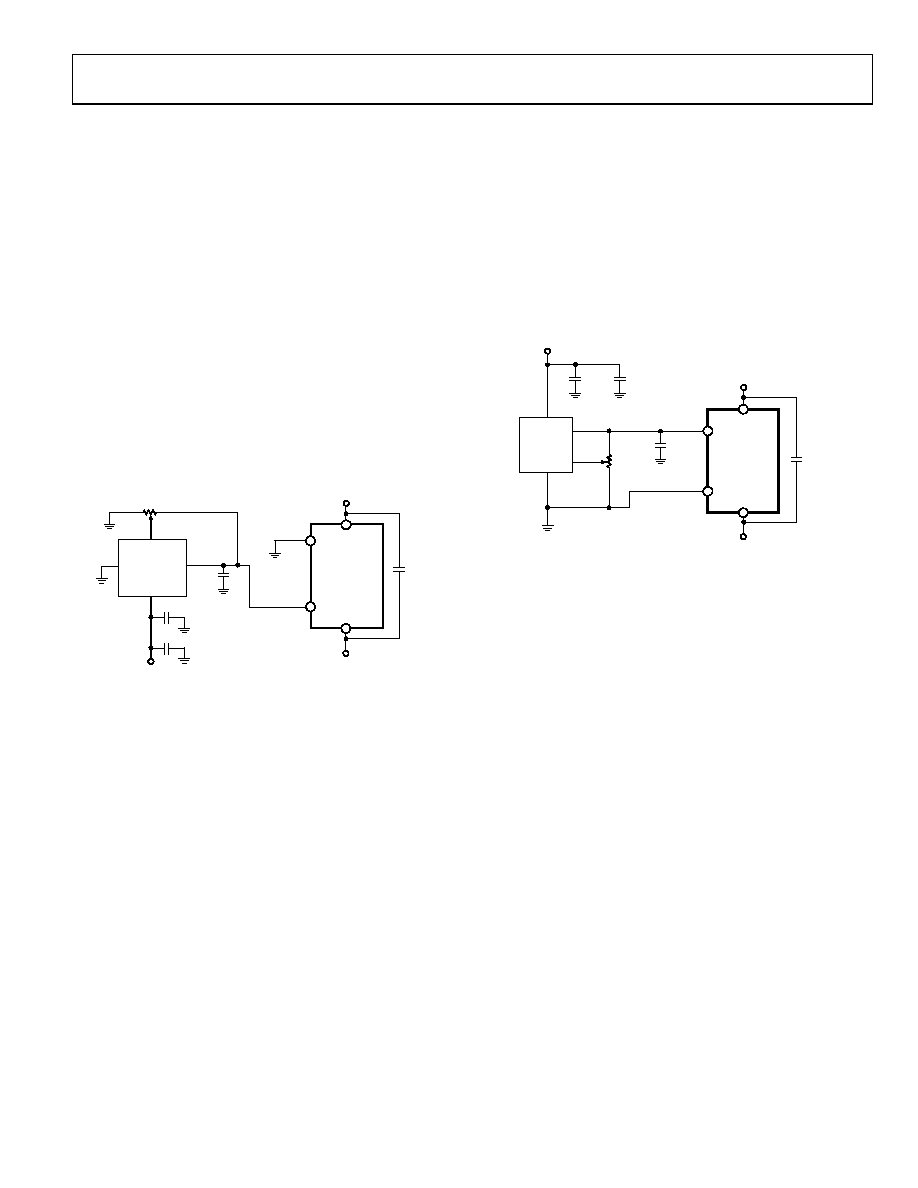
10k
0.01F
10F
–15V
GND
TRIM
OUTPUT
VOLTAGE
REFERENCE
0.2F
VREFL
VREFH
DAC8412
OR
DAC8413
0.1F
//10F
ZERO TO –10V OPERATION
VDD
VSS
0
027
4-
0
42
Figure 41. Unipolar –10 V Operation
Figure 41 shows the DAC8412 configured for –10 V to 0 V
operation. A –10 V full-scale output voltage reference is
connected directly to VREFL for the reference voltage.
SINGLE +5 V SUPPLY OPERATION
For operation with a 5 V supply, the reference voltage should be
set between 1.0 V and 2.5 V for optimum linearity. Figure 42
shows a REF43 used to supply a 2.5 V reference voltage. The
headroom of the reference and DAC are both sufficient to support
a 5 V supply with ±5% tolerance. VDD and VLOGIC should be
connected to the same supply. Separate bypassing to each pin
should also be used.
5V
INPUT
OUTPUT
GND
TRIM
REF43
ZERO TO 2.5V OPERATION
SINGLE 5V SUPPLY
10k
0.2F
VREFL
VREFH
DAC8412
OR
DAC8413
0.1F
//10F
10F
0.01F
VDD
VSS
00
27
4-
0
43
Figure 42. +5 V Single-Supply Operation
相关PDF资料 |
PDF描述 |
|---|---|
| VE-JWJ-MW-S | CONVERTER MOD DC/DC 36V 100W |
| AD5764RCSUZ-REEL7 | IC DAC QUAD 16BIT VOUT 32-TQFP |
| VE-JWH-MW-S | CONVERTER MOD DC/DC 52V 100W |
| LTC2758BILX#PBF | IC DAC 18BIT SPI/SRL 48-LQFP |
| AD569JPZ-REEL | IC DAC 16BIT MONO NON-LIN 28PLCC |
相关代理商/技术参数 |
参数描述 |
|---|---|
| DAC8412FT | 制造商:Rochester Electronics LLC 功能描述:- Bulk |
| DAC8412FTC | 制造商:未知厂家 制造商全称:未知厂家 功能描述:12-Bit Digital-to-Analog Converter |
| DAC8413 | 制造商:AD 制造商全称:Analog Devices 功能描述:Quad, 12-Bit DAC Voltage Output with Readback |
| DAC8413AT/883 | 制造商:未知厂家 制造商全称:未知厂家 功能描述:12-Bit Digital-to-Analog Converter |
| DAC8413AT/883C | 功能描述:数模转换器- DAC QUAD 12-BIT VOUT DAC-LEV. B RoHS:否 制造商:Analog Devices 转换器数量:4 DAC 输出端数量:4 转换速率:167 Ksps 分辨率:12 bit 接口类型:Parallel 稳定时间:10 us (Typ) 最大工作温度:+ 125 C 安装风格: 封装 / 箱体:CDIP 封装:Tube |
发布紧急采购,3分钟左右您将得到回复。